LTC6803-2/LTC6803-4
28
680324fa
APPLICATIONS INFORMATION
DIFFERENCE BETWEEN THE LTC6803-2 AND LTC6803-4
The only difference between the LTC6803-2 and the
LTC6803-4 is the bonding of the V
and C0 pins. The
V
and C0 are separate signals on every LTC6803 die.
In the LTC6803-2 package, the V
and C0 signals are
shorted together by bonding these signals to the same
pin. In the LTC6803-4 package, V
and C0 are separate
pins. Therefore, the LTC6803-2 is pin compatible with the
LTC6802-2. For new designs the LTC6803-4 pinout allows
a Kelvin connection to C0 (Figure 22).
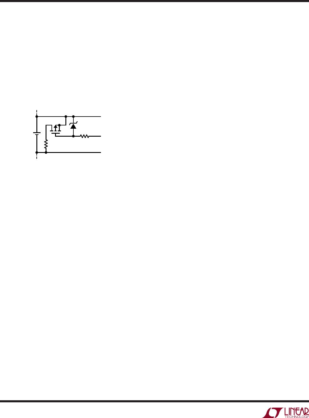
CELL VOLTAGE FILTERING
The LTC6803 employs a sampling system to perform its
analog-to-digital conversions and provides a conversion
result that is essentially an average over the 0.5ms con-
version window, provided there isn’t noise aliasing with
respect to the delta-sigma modulator rate of 512kHz. This
indicates that a lowpass filter with 30dB attenuation at
500kHz may be beneficial. Since the delta-sigma integra-
tion bandwidth is about 1kHz, the filter corner need not
be lower than this to assure accurate conversions.
Series resistors of 100Ω may be inserted in the input
paths without introducing meaningful measurement er-
ror. Shunt capacitors may be added from the cell inputs
to V
, creating RC filtering as shown in Figure 8. The cell
balancing MOSFET in Figure 11 can cause a small transient
when it switches on and off. Keeping the cutoff frequency
of the RC filter relatively high will allow adequate settling
prior to the actual conversion. A delay of about 500µs is
provided in the ADC timing, so a 16kHz LPF is optimal
(100Ω, 0.1µF) and offers about 30dB of noise rejection.
Larger series resistors and shunt capacitors can be used
to lower the filter bandwidth. The measurement error due
to the larger component values is a complex function of
the component values. The error also depends on how
often measurements are made. Table 17 is an example. In
each example a 3.6V cell is being measured and the error
is displayed in millivolts. There is a RC filter in series with
inputs C1 through C12. There is no filter in series with
C0. There is an interaction between cells. This is why the
errors for C1 and C12 differ from C2 through C11.
Table 17. Cell Measurement Errors vs Input RC Values
R = 100Ω,
C = 0.1µF
R = 1k,
C = 0.1µF
R = 1k,
C = 1µF
R = 10k,
C = 3.3µF
Cell 1 Error
(mV, LTC6803-2)
0.1 4.5 1.5 1.5
Cell 2 to Cell 12 (mV) 1 9 3 0.5
For the LTC6803-2, no resistor should be placed in series
with the V
pin. Because the supply current flows from
the V
pin, any resistance on this pin could generate a
significant conversion error for cell 1, and the error of
cell 1 caused by the RC filter differs from errors of cell 2
to cell 2.
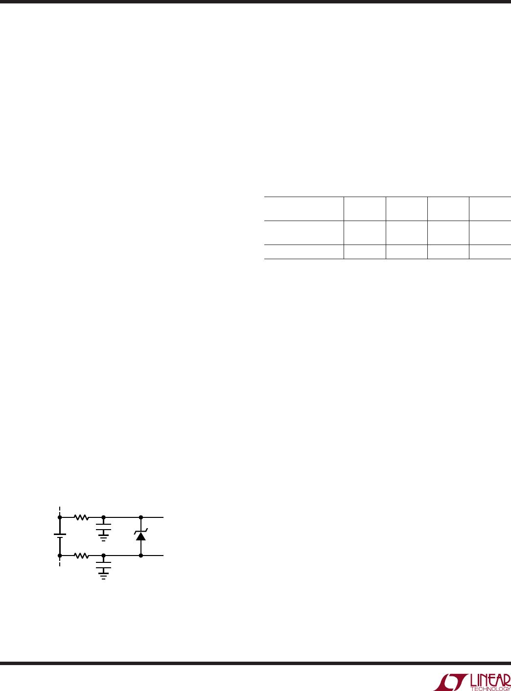
OPEN-CONNECTION DETECTION
When a cell input (C pin) is open, it affects two cell mea-
surements. Figure 9 shows an open connection to C3,
in an application without external filtering between the C
pins and the cells. During normal ADC conversions (that
is, using the STCVAD command), the LTC6803 will give
near zero readings for B3 and B4 when C3 is open. The
zero reading for B3 occurs because during the measure-
ment of B3, the ADC input resistance will pull C3 to the
C2 potential. Similarly, during the measurement of B4, the
ADC input resistance pulls C3 to the C4 potential.
Figure 10 shows an open connection at the same point in
the cell stack as Figure 9, but this time there is an external
filtering network still connected to C3. Depending on the
value of the capacitor remaining on C3, a normal measure-
ment of B3 and B4 may not give near-zero readings, since
the C3 pin is not truly open. In fact, with a large external
capacitance on C3, the C3 voltage will be charged midway
Figure 8. Adding RC Filtering to the Cell Inputs
(One Cell Connection Shown)
+
100nF
100nF
680324 F08
7.5V
Cn
C(n – 1)
100Ω
100Ω
LTC6803-2/LTC6803-4
29
680324fa
APPLICATIONS INFORMATION
Figure 9. Open Connection
Figure 10. Open Connection with RC Filtering
between C2 and C4 after several cycles of measuring cells
B3 and B4. Thus the measurements for B3 and B4 may
indicate a valid cell voltage when in fact the exact state of
B3 and B4 is unknown.
To reliably detect an open connection, the command
STOWAD is provided. With this command, two 100µA
current sources are connected to the ADC inputs and
turned on during all cell conversions. Referring again to
Figure 10, with the STOWAD command, the C3 pin will be
pulled down by the 100µA current source during the B3
cell measurement AND during the B4 cell measurement.
This will tend to decrease the B3 measurement result and
increase the B4 measurement result relative to the normal
STCVAD command. The biggest change is observed in the
B4 measurement when C3 is open. So, the best method to
detect an open wire at input C3 is to look for an increase
in the value of battery connected between inputs C3 and
C4 (battery B4).
The following algorithm can be used to detect an open
connection to cell pin Cn:
1. Issue a STOWAD command (with 100µA sources
connected).
2. Issue a RDCV command and store all cell measurements
into array CELLA(n).
3. Issue the 2nd STOWAD command (with 100µA sources
connected).
4. Issue the 2nd RDCV command and store all cell mea-
surements into array CELLB(n).
5. For battery cells, if CELLA(1) < 0 or CELLB(1) < 0, V
must be open.
If CELLA(12) < 0 or CELLB(12) < 0, C12 must be open.
For n = 2 to 11, if CELLB(n+1) – CELLA(n+1) > 200mV,
or CELLB(n+1) reaches the full scale of 5.375V, then
Cn is open.
The 200mV threshold is chosen to provide tolerance for
measurement errors. For a system with the capacitor con-
nected to Cn larger than 0.5µF, repeating step 3 several
times will discharge the external capacitor enough to meet
the criteria.
If the top C pin is open yet V
+
is still connected, then the
best way to detect an open connection to the top C pin
is by comparing the sum of all cell measurements using
the STCVAD command to an auxiliary measurement of
the sum of all the cells, using a method similar to that
shown in Figure 19. A significantly lower result for the
sum of all 12 cells suggests an open connection to the
top C pin, provided it was already determined that no
other C pin is open.
+
+
+
+
+
100µA
MUX
C2
22
C3
20
C4
B4
B3
680324 F09
LTC6803-4
18
V
1
C1
24
+
+
+
+
+
100µA
MUX
C2
22
C3
20
C4
B4 C
F4
C
F3
B3
680324 F10
LTC6803-4
18
V
1
C1
24
LTC6803-2/LTC6803-4
30
680324fa
USING THE S PINS AS DIGITAL OUTPUTS OR GATE
DRIVERS
The S outputs include an internal pull-up PMOS. Therefore
the S pins will behave as a digital output when loaded with
a high impedance, e.g. the gate of an external MOSFET.
For applications requiring high battery discharge currents,
connect a discrete PMOS switch device and suitable dis-
charge resistor to the cell, and the gate terminal to the S
output pin, as illustrated in Figure 11.
detected on the device goes above approximately 145°C,
the configuration registers will be reset to default states,
turning off all discharge switches and disabling ADC
conversions. When a thermal shutdown has occurred, the
THSD bit in the temperature register group will go high.
The bit is cleared by performing a read of the temperature
registers (RDTMP command).
Since thermal shutdown interrupts normal operation, the
internal temperature monitor should be used to determine
when the device temperature is approaching unacceptable
levels.
USING THE LTC6803 WITH LESS THAN 12 CELLS
If the LTC6803 is powered by the stacked cells, the minimum
number of cells is governed by the supply voltage require-
ments of the LTC6803. The sum of the cell voltages must be
10V to guarantee that all electrical specifications are met.
Figure 12 shows an example of the LTC6803-4 when used
to monitor seven cells. The lowest C inputs connect to the
seven cells and the upper C inputs connect to C12. Other
configurations, e.g., 9 cells, would be configured in the
same way: the lowest C inputs connected to the battery
cells and the unused C inputs connected to C12. The unused
inputs will result in a reading of 0V for those channels.
The ADC can also be commanded to measure a stack of
10 or 12 cells, depending on the state of the CELL10 bit
in the control register. The ADC can also be commanded
to measure any individual cell voltage.
FAULT PROTECTION
Care should always be taken when using high energy
sources such as batteries. There are numerous ways
that systems can be (mis)configured when considering
the assembly and service procedures that might affect a
battery system during its useful lifespan. Table 18 shows
the various situations that should be considered when plan-
ning protection circuitry. The first five scenarios are to be
anticipated during production and appropriate protection
is included within the LTC6803 device itself.
APPLICATIONS INFORMATION
Figure 11. External Discharge FET Connection (One Cell Shown)
+
680324 F11
Cn
Cn – 1
Sn
3.3k
33Ω
1W
Si2351DS
POWER DISSIPATION AND THERMAL SHUTDOWN
The MOSFETs connected to the Pins S1 through S12 can be
used to discharge battery cells. An external resistor should
be used to limit the power dissipated by the MOSFETs. The
maximum power dissipation in the MOSFETs is limited by
the amount of heat that can be tolerated by the LTC6803.
Excessive heat results in elevated die temperatures. The
electrical characteristics for the LTC6803 I-grade are
guaranteed for die temperatures up to 85°C. Little or no
degradation will be observed in the measurement accuracy
for die temperatures up to 105°C. Damage may occur
above 150°C, therefore the recommended maximum die
temperature is 125°C.
To protect the LTC6803 from damage due to overheating,
a thermal shutdown circuit is included. Overheating of the
device can occur when dissipating significant power in
the cell discharge switches. The problem is exacerbated
when operating with a large voltage between V
+
and V
.
The thermal shutdown circuit is enabled whenever the
device is not in standby mode (see Modes of Operation).
It will also be enabled when any current mode input or
output is sinking or sourcing current. If the temperature

LTC6803HG-2#PBF

Mfr. #:
Manufacturer:
Analog Devices / Linear Technology
Description:
Battery Management Battery Stack Monitor, Addressable SPI
Lifecycle:
New from this manufacturer.
Delivery:
DHL FedEx Ups TNT EMS
Payment:
T/T Paypal Visa MoneyGram Western Union