LTC6803-2/LTC6803-4
4
680324fa
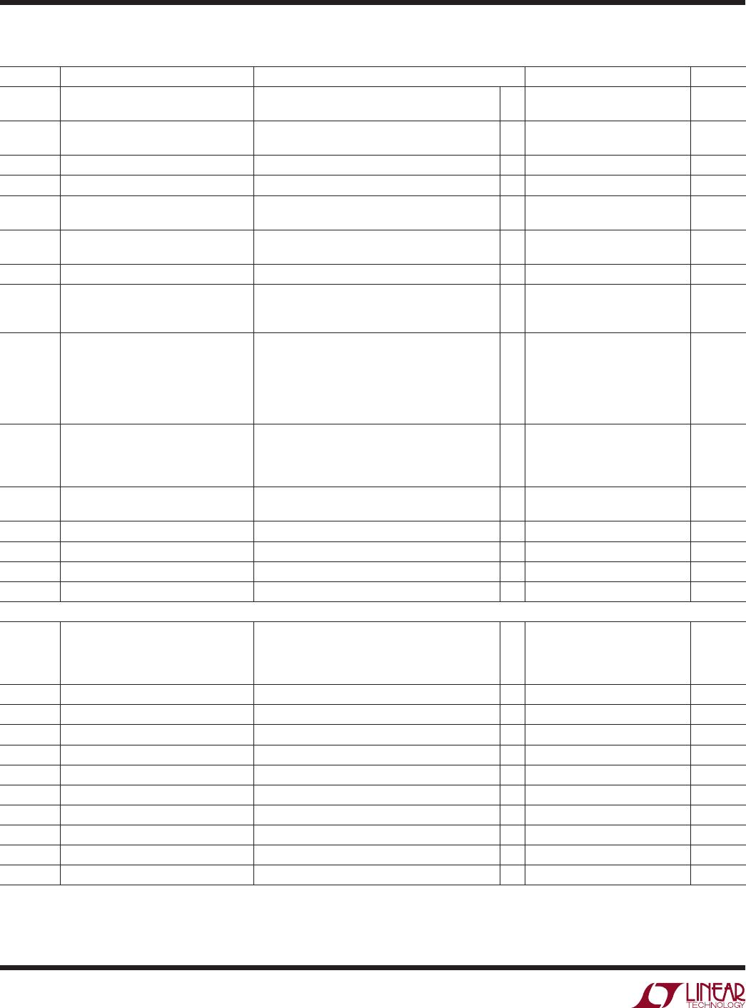
ELECTRICAL CHARACTERISTICS
The l denotes the specifications which apply over the full operating
temperature range, otherwise specifications are at T
A
= 25°C. V
+
= 43.2V, V
= 0V, unless otherwise noted.
SYMBOL PARAMETER CONDITIONS MIN TYP MAX UNITS
V
REF
Reference Pin Voltage R
LOAD
= 100k to V
l
3.020
3.015
3.065
3.065
3.110
3.115
V
V
Reference Voltage Temperature
Coefficient
8 ppm/°C
Reference Voltage Thermal Hysteresis 25°C to 85°C and 25°C to –40°C 100 ppm
Reference Voltage Long-Term Drift 60 ppm/√kHr
V
REF2
2nd Reference Voltage
l
2.25
2.1
2.5
2.5
2.75
2.9
V
V
V
REG
Regulator Pin Voltage 10V < V
+
< 50V, No Load
I
LOAD
= 4mA
l
l
4.5
4.5
5.0
5.0
5.5 V
V
Regulator Pin Short-Circuit Limit
l
8 mA
I
B
Input Bias Current In/Out of Pins C1 Through C12
When Measuring Cell
When Not Measuring Cell
–10
1
10
µA
nA
I
S
Supply Current, Measure Mode
(Note 7)
Current Into the V
+
Pin When Measuring
Continuous Measuring (CDC = 2)
Measure Every 130ms (CDC = 5)
Measure Every 500ms (CDC = 6)
Measure Every 2 Seconds (CDC = 7)
l
l
l
l
620
600
190
140
55
780
780
250
175
70
1000
1150
360
250
105
µA
µA
µA
µA
µA
I
QS
Supply Current, Standby Current Into V
+
Pin When In Standby, All Serial
Port Pin at Logic “1”
LTC6803IG
LTC6803HG
l
l
8
6
6
12
12
12
16.5
18
19
µA
µA
µA
I
SD
Supply Current, Hardware Shutdown Current Out of V
, V
C12
= 43.2V, V
+
Floating
(Note 8)
l
0.001 1 µA
Discharge Switch-On Resistance V
CELL
> 3V (Note 3)
l
10 20 Ω
I
OW
Current Used for Open-Wire Detection
l
70 110 140 µA
Thermal Shutdown Temperature 145 °C
Thermal Shutdown Hysteresis 5 °C
Voltage Mode Timing Specifications
t
CYCLE
Measurement Cycling Time Required to Measure 12 Cells
Time Required to Measure 10 Cells
Time Required to Measure 3 Temperatures
Time Required to Measure 1 Cell or Temperature
l
l
l
l
11
9
2.8
1.0
13
11
3.4
1.2
15
13
4.1
1.4
ms
ms
ms
ms
t
1
SDI Valid to SCKI Rising Setup
l
10 ns
t
2
SDI Valid to SCKI Rising Hold
l
250 ns
t
3
SCKI Low
l
400 ns
t
4
SCKI High
l
400 ns
t
5
CSBI Pulse Width
l
400 ns
t
6
CSBI Falling to SCKI Rising
l
100 ns
t
7
CSBI Falling to SDO Valid
l
100 ns
t
8
SCKI Falling to SDO Valid
l
250 ns
Clock Frequency
l
1 MHz
Watchdog Timer Timeout Period
l
1 2.5 Seconds
LTC6803-2/LTC6803-4
5
680324fa
Note 1: Stresses beyond those listed under Absolute Maximum Ratings
may cause permanent damage to the device. Exposure to any Absolute
Maximum Rating condition for extended periods may affect device
reliability and lifetime.
Note 2: The ADC specifications are guaranteed by the Total Measurement
Error (V
ERR
) specification.
Note 3: Due to the contact resistance of the production tester, this
specification is tested to relaxed limits. The 20Ω limit is guaranteed by
design.
Note 4: V
CELL
refers to the voltage applied across Cn to Cn – 1 for
n = 1 to 12. V
TEMP
refers to the voltage applied from V
TEMP1
or V
TEMP2
to V
.
Note 5: These absolute maximum ratings apply provided that the voltage
between inputs do not exceed the absolute maximum ratings.
Note 6: Supply current is tested during continuous measuring. The supply
current during periodic measuring (130ms, 500ms, 2s) is guaranteed by
design.
Note 7: The CDC = 5, 6 and 7 supply currents are not measured. They are
guaranteed by the CDC = 2 supply current measurement.
Note 8: Limit is determined by high speed automated test capability.
ELECTRICAL CHARACTERISTICS
The l denotes the specifications which apply over the full operating
temperature range, otherwise specifications are at T
A
= 25°C. V
+
= 43.2V, V
= 0V, unless otherwise noted.
SYMBOL PARAMETER CONDITIONS MIN TYP MAX UNITS
Voltage Mode Digital I/O
V
IH
Digital Input Voltage High Pins SCKI, SDI and CSBI
l
2 V
V
IL
Digital Input Voltage Low Pins SCKI, SDI and CSBI
l
0.8 V
V
OL
Digital Output Voltage Low Pin SDO, Sinking 500µA
l
0.3 V
I
IN
Digital Input Current V
MODE
, TOS, SCKI, SDI, CSBI
l
10 µA
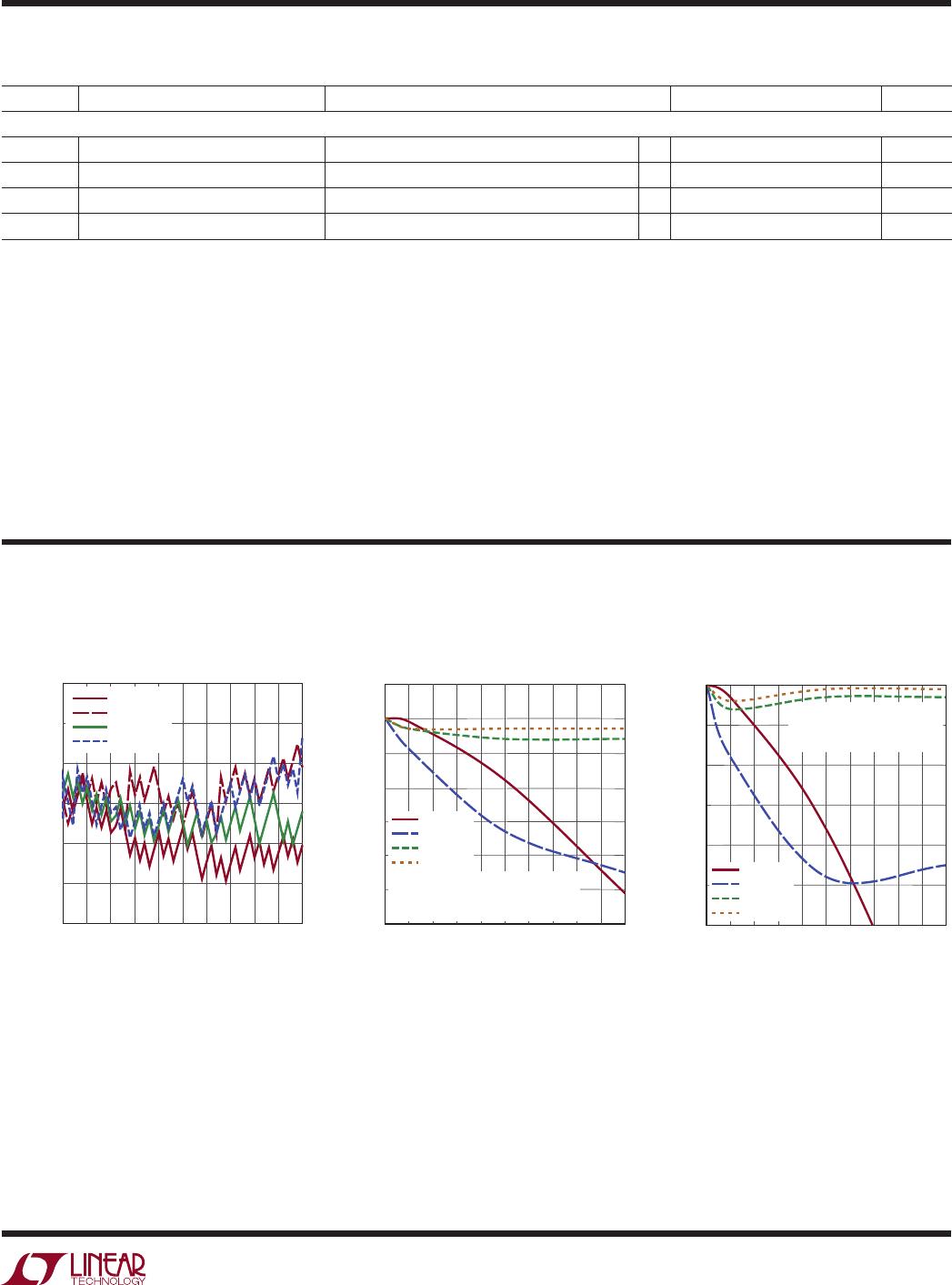
TYPICAL PERFORMANCE CHARACTERISTICS
Cell Measurement Error
vs Cell Input Voltage
Cell Measurement Error
vs Input RC Values
Cell Measurement Error
vs Input RC Values
CELL INPUT VOLTAGE (V)
–4.5
TOTAL UNADJUSTED ERROR (mV)
–1.5
1.5
4.5
–3.0
0
3.0
1.0 2.0 3.0 4.0
680324 G01
5.00.50 1.5 2.5 3.5 4.5
T
A
= 125°C
T
A
= 85°C
T
A
= 25°C
T
A
= –40°C
INPUT RESISTANCE (kΩ)
0
–30
CELL VOLTAGE ERROR (mV)
–25
–15
–10
–5
5
1
5
7
680324 G02
–20
0
4
9
10
2
3
6 8
C = 0µF
C = 0.1µF
C = 1µF
C = 3.3µF
CELL 1, 13ms CELL MEASUREMENT
REPETITION
V
CELL
= 3.3V
INPUT RESISTANCE (kΩ)
0
–30
CELL VOLTAGE ERROR (mV)
–25
–15
–10
–5
0
1
5
7
680324 G03
–20
4
9
10
2
3
6 8
C = 0µF
C = 0.1µF
C = 1µF
C = 3.3µF
CELLS 2 TO 12, 13ms CELL
MEASUREMENT REPETITION
V
CELL
= 3.3V
LTC6803-2/LTC6803-4
6
680324fa
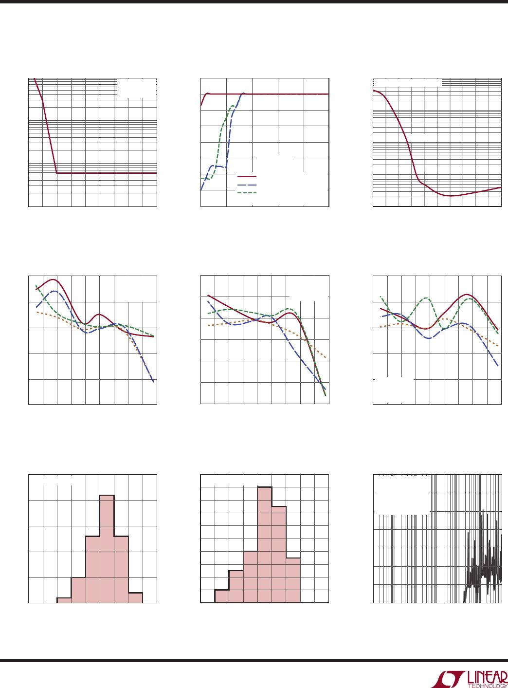
TYPICAL PERFORMANCE CHARACTERISTICS
Cell Voltage Measurement Error
vs Common Mode Voltage
Cell Measurement Error
vs Cell Voltage
Cell 1 Voltage Measurement Error
vs Temperature
Cell 12 Measurement Error vs V
+
Cell 2 Voltage Measurement Error
vs Temperature
Cell 3 to Cell 12 Voltage
Measurement Error vs Temperature
Measurement Gain Error
Hysteresis
Cell Measurement Common Mode
Rejection
Measurement Gain Error
Hysteresis
V
+
– V
C12
(V)
–0.8
–0.6 –0.4
CELL 12 MEASUREMENT ERROR (mV)
1
10
100
–0.2 0 0.2 0.4 0.6 1.00.8
680324 G04
0.1
T
A
= 25°C
V
CELL
= 3.3V
COMMON MODE VOLTAGE (V)
0
CELL MEASUREMENT ERROR (mV)
–8
–6
–4
3
5
680324 G05
–10
–12
–14
1 2 4
–2
0
2
CELL2 ERROR vs V
C1
CELL3 ERROR vs V
C2
CELLn ERROR VS V
Cn–1
,
n = 4 TO 12
V
CELL
= 3.6V
T
A
= 25°C
V
IN
CELL6 (V)
1
CELL VOLTAGE MEASUREMENT ERROR (mV)
10
100
1000
–1.0 –0.2 0.2 0.6
0.1
–0.6
1.0–0.4 0 0.4–0.8 0.8
680324 G06
CELL6
ALL OTHER CELLS = 3V
TEMPERATURE (°C)
–50
–2.00
CELL MEASUREMENT ERROR (mV)
–1.25
0.25
1.00
1.75
–10
30
50 130
680324 G07
–0.50
–30 10
70
90
110
V
CELL
= 0.8V
V
+
= 9.6V
4 SAMPLES
TEMPERATURE (°C)
–50
–2.00
CELL MEASUREMENT ERROR (mV)
–1.25
0.25
1.00
2.50
1.75
–10
30
50 130
680324 G08
–0.50
–30 10
70
90
110
V
CELL
= 0.8V
V
+
= 9.6V
4 SAMPLES
TEMPERATURE (°C)
–50
–2.00
CELL MEASUREMENT ERROR (mV)
–1.25
0.25
1.00
1.75
–10
30
50 130
680324 G09
–0.50
–30 10
70
90
110
V
CELL
= 0.8V
V
+
= 9.6V
4 SAMPLES
CHANGE IN GAIN ERROR (ppm)
–250
NUMBER OF UNITS
25
20
15
10
5
0
–50 150–150 50
680324 G10
200–100 100–200 0
T
A
= 85°C TO 25°C
CHANGE IN GAIN ERROR (ppm)
–250
NUMBER OF UNITS
20
16
12
8
4
18
14
10
6
2
0
–50 150–150 50
680324 G11
200–100 100–200 0
T
A
= –45°C TO 25°C
0
–10
–30
–50
–20
–40
–60
–70
FREQUENCY (Hz)
REJECTION (dB)
680324 G12
10 10k 10M1M100k1k100
V
CM(IN)
= 5V
P-P
72dB REJECTION
CORRESPONDS TO
LESS THAN 1 BIT
AT ADC OUTPUT

LTC6803HG-2#PBF

Mfr. #:
Manufacturer:
Analog Devices / Linear Technology
Description:
Battery Management Battery Stack Monitor, Addressable SPI
Lifecycle:
New from this manufacturer.
Delivery:
DHL FedEx Ups TNT EMS
Payment:
T/T Paypal Visa MoneyGram Western Union