LTC6803-2/LTC6803-4
36
680324fa
APPLICATIONS INFORMATION
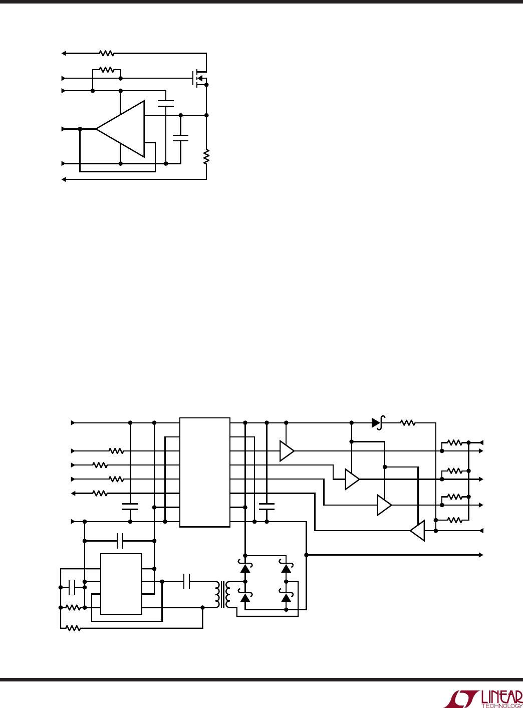
HARDWARE SHUTDOWN
To completely shut down the LTC6803 a PMOS switch can
be connected to V
+
, or, V
+
can be driven from an isolated
power supply. Figure 23 shows an example of a switched
V
+
. The breakdown voltage of DZ4 is about 1.8V. If SHDN <
1.8V, no current will flow through the stacked MMBTA42s
and the 1M resistors. TP0610Ks will be completely shut
off. If SHDN > 2.5V, M7 will be turned on and then all
TP0610Ks will be turned on.
separation of traces at different potentials. The pinout
of the LTC6803 was chosen to facilitate this physical
separation. There is no more than 5.5V between any two
adjacent pins. The package body is used to separate the
highest voltage (e.g., 43.2V) from the lowest voltage (0V).
As an example, Figure 24 shows the DC voltage on each
pin with respect to V
–
when twelve 3.6V battery cells are
connected to the LTC6803.
Figure 24. Typical Pin Voltages for Twelve 3.6V Cells
Figure 23. Hardware Shutdown Circuit Reduces Total Supply
Current of LTC6803-4 to About 0µA
TP0610K
DZ3
15V
DZ4
1.8V
DZ1, DZ2, DZ3: MMSZ5245B
DZ4: MMSZ4678T1
ALL NPN: MMBTA42
ALL PN: RS07J
1M
50k
680324 F23
SHDN
V
+
V
–
C0
C12
LTC6803-4
IC #1
TP0610K
DZ2
15V
1M
D2
V
+
V
–
C0
C12
LTC6803-4
IC #2
TP0610K
DZ1
15V
1M
D1
V
+
V
–
C0
C12
LTC6803-4
IC #3
+
+
+
+
+
+
+
+
+
V
+
C12
S12
C11
S11
C10
S10
C9
S9
C8
S8
C7
S7
C6
S6
C5
S5
C4
S4
C3
S3
C2
CSBI
SDO
SDI
SCKI
A3
A2
A1
A0
GPIO2
GPIO1
WDTB
TOS
V
REG
V
REF
V
TEMP2
V
TEMP1
NC
V
–
C0
S1
C1
S2
43.2V
43.2V
43.2V
39.6V
39.6V
36V
36V
32.4V
32.4V
28.8V
28.8V
25.2V
25.2V
21.6
21.6
18V
18V
14.4V
14.4V
10.8
10.8
7.2
0V TO 5.5V
0V TO 5.5V
0V TO 5.5V
0V TO 5.5V
0V TO 5.5V
0V TO 5.5V
0V TO 5.5V
0V TO 5.5V
0V TO 5.5V
0V TO 5.5V
0V TO 5.5V
0V TO 5.5V
5V
3.1V
1.5V
1.5V
0V
0V
0V
3.6V
3.6V
7.2V
LTC6803-4
680324 F24
PCB LAYOUT CONSIDERATIONS
The V
REG
and V
REF
pins should be bypassed with a 1µF
capacitor for best performance. The LTC6803 is capable of
operation with as much as 55V between V
+
and V
–
. Care
should be taken on the PCB layout to maintain physical
ADVANTAGES OF DELTA-SIGMA ADCS
The LTC6803 employs a delta-sigma analog-to-digital
converter for voltage measurement. The architecture of
delta-sigma converters can vary considerably, but the
common characteristic is that the input is sampled many
times over the course of a conversion and then filtered or
averaged to produce the digital output code. In contrast,
a SAR converter takes a single snapshot of the input
voltage and then performs the conversion on this single
sample. For measurements in a noisy environment, a
delta-sigma converter provides distinct advantages over
a SAR converter.
While SAR converters can have high sample rates, the full-
power bandwidth of a SAR converter is often greater than