LTC6803-2/LTC6803-4
31
680324fa
APPLICATIONS INFORMATION
Table 18. LTC6803 Failure Mechanism Effect Analysis
SCENARIO EFFECT DESIGN MITIGATION
Cell input open-circuit (random) Power-up sequence at IC inputs Clamp diodes at each pin to V
+
and V
–
(within IC) provide
alternate power path
Cell input open-circuit (random) Differential input voltage overstress Zener diodes across each cell voltage input pair (within IC) limits
stress
Disconnection of a harness between
a group of battery cells and the IC
(in a system of stacked groups)
Loss of supply connection to the IC Separate power may be provided by a local supply
Data link disconnection between
LTC6803 and the master
Loss of serial communication (no stress to ICs) The device will enter standby mode within 2 seconds of
disconnect. Discharge switches are disabled in standby mode
Cell-pack integrity, break between
stacked units
No effect during charge or discharge Use digital isolators to isolate the LTC6803-2/LTC6803-4 serial
port from other LTC6803-2/LTC6803-4 serial ports
Cell-pack integrity, break within
stacked unit
Cell input reverse overstress during discharge Add parallel Schottky diodes across each cell for load-path
redundancy. Diode and connections must handle full operating
current of stack, will limit stress on IC
Cell-pack integrity, break within
stacked unit
Cell input positive overstress during charge Add SCR across each cell for charge-path redundancy. SCR and
connections must handle full charging current of stack, will limit
stress on IC by selection of trigger Zener
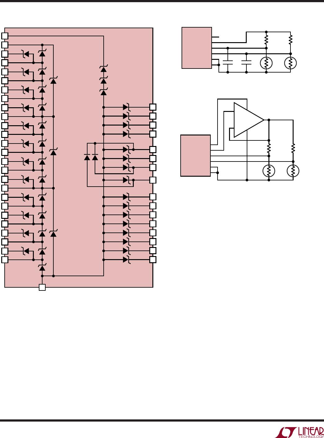
Internal Protection Diodes
Each pin of the LTC6803 has protection diodes to help
prevent damage to the internal device structures caused
by external application of voltages beyond the supply rails
as shown in Figure 13. The diodes shown are conventional
silicon diodes with a forward breakdown voltage of 0.5V.
The unlabeled Zener diode structures have a reverse
breakdown characteristic which initially breaks down at
12V then snaps back to a 7V clamping potential. The Zener
diodes labeled Z
CLAMP
are higher voltage devices with an
initial reverse breakdown of 30V snapping back to 25V.
The forward voltage drop of all Zeners is 0.5V. Refer to
this diagram in the event of unpredictable voltage clamp-
ing or current flow. Limiting the current flow at any pin to
±10mA will prevent damage to the IC.
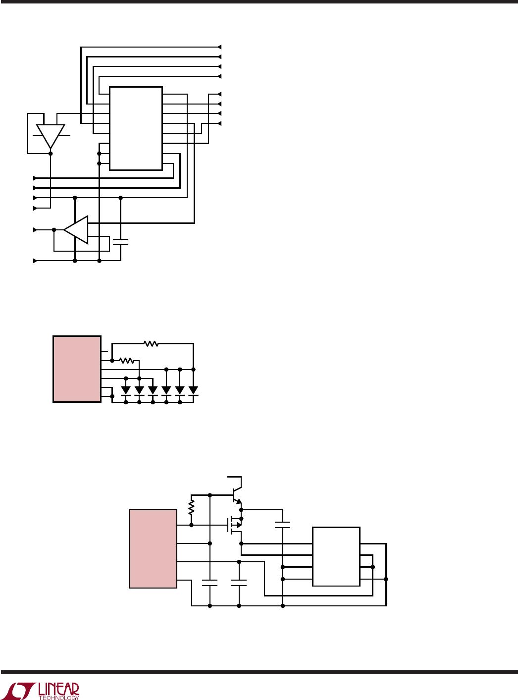
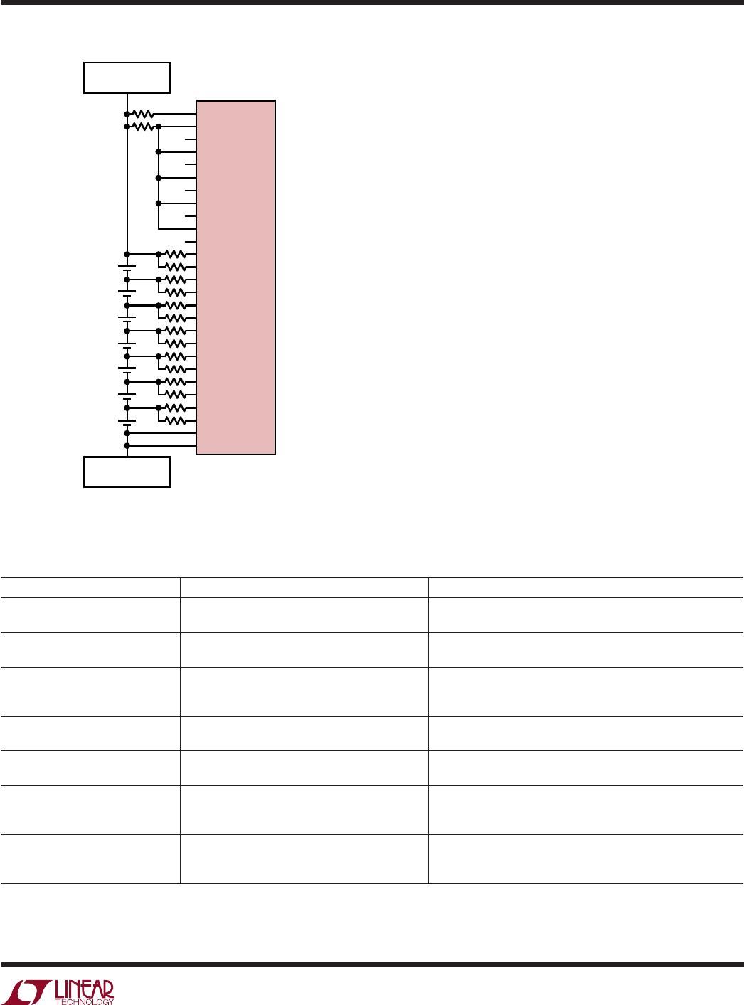
READING EXTERNAL TEMPERATURE PROBES
The LTC6803 includes two channels of ADC input, V
TEMP1
and V
TEMP2
, that are intended to monitor thermistors
(tempco about –4%/°C generally) or diodes (–2.2mV/°C
typical) located within the cell array. Sensors can be
powered directly from V
REF
as shown in Figure 14 (up to
60µA total).
+
+
+
+
+
+
+
V
+
C12
S12
C11
S11
C10
S10
C9
S9
C8
S8
C7
S7
C6
S6
C5
S5
C4
S4
C3
S3
C2
S2
C1
S1
C0
V
–
LTC6803-4
100
NEXT HIGHER GROUP
OF 7 CELLS
NEXT LOWER GROUP
OF 7 CELLS
680324 F12
Figure 12. Monitoring 7 Cells with the LTC6803-4