MT9V024/D
www.onsemi.com
10
clocks out the register data 8 bits at a time. The master sends
an acknowledge bit after each 8bit transfer. The register
address is automatically incremented after every 16 bits is
transferred. The data transfer is stopped when the master
sends a noacknowledge bit. The MT9V024 allows for 8bit
data transfers through the twowire serial interface by
writing (or reading) the most significant 8 bits to the register
and then writing (or reading) the least significant 8 bits to
bytewise address register (0x0F0).
Bus Idle State
The bus is idle when both the data and clock lines are
HIGH. Control of the bus is initiated with a start bit, and the
bus is released with a stop bit. Only the master can generate
the start and stop bits.
Table 6. SLAVE ADDRESS MODES
{S_CTRL_ADR1, S_CTRL_ADR0} Slave Address Write/Read Mode
00
0x90 Write
0x91 Read
01
0x98 Write
0x99 Read
10
0xB0 Write
0xB1 Read
11
0xB8 Write
0xB9 Read
Data Bit Transfer
One data bit is transferred during each clock pulse. The
twowire serial interface clock pulse is provided by the
master. The data must be stable during the HIGH period of
the serial clockit can only change when the twowire serial
interface clock is LOW. Data is transferred 8 bits at a time,
followed by an acknowledge bit.
TWOWIRE SERIAL INTERFACE SAMPLE READ AND WRITE SEQUENCES
16Bit Write Sequence
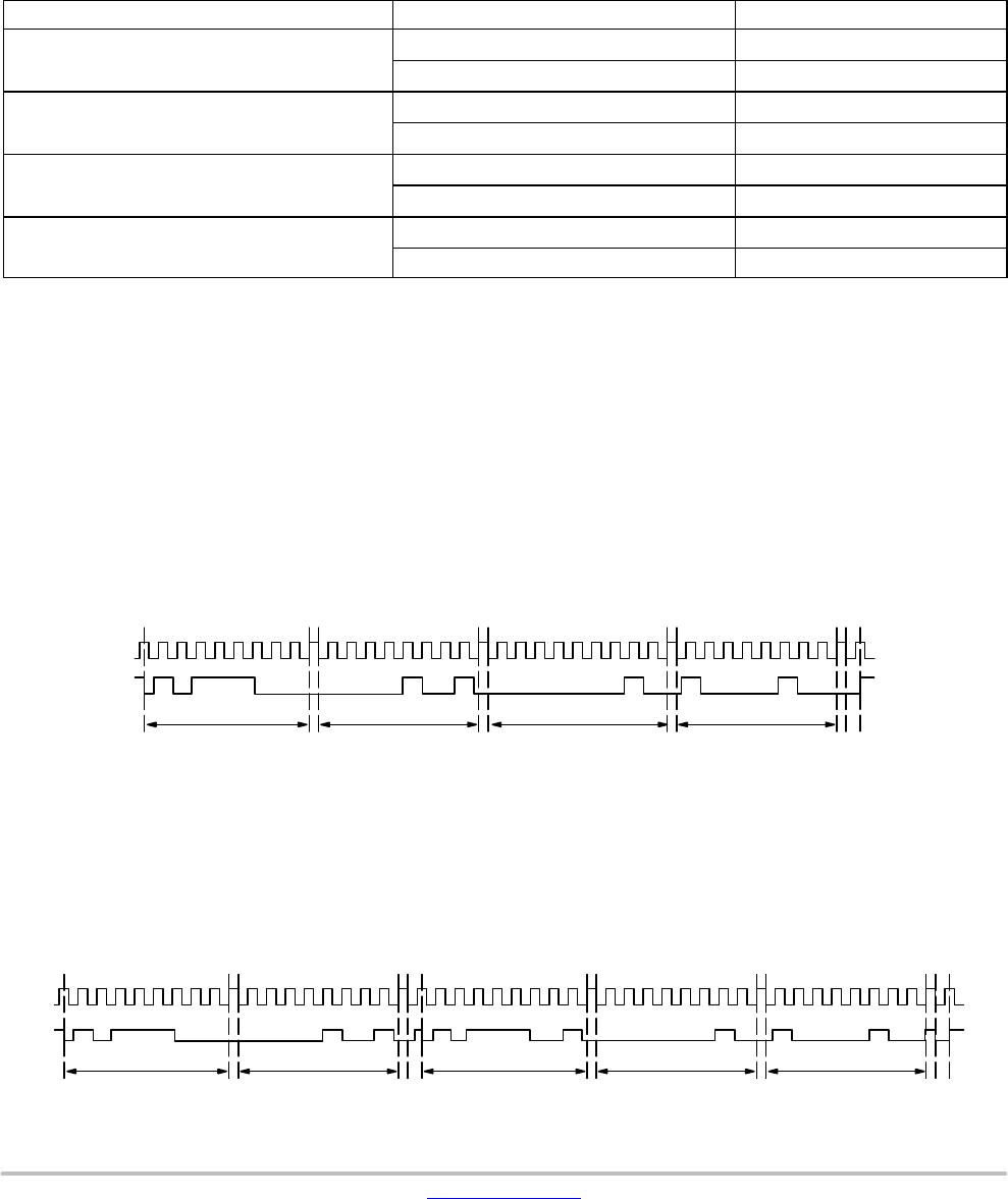
A typical write sequence for writing 16 bits to a register
is shown in Figure 10. A start bit given by the master,
followed by the write address, starts the sequence. The
image sensor then gives an acknowledge bit and expects the
register address to come first, followed by the 16bit data.
After each 8bit word is sent, the image sensor gives an
acknowledge bit. All 16 bits must be written before the
register is updated. After 16 bits are transferred, the register
address is automatically incremented, so that the next 16 bits
are written to the next register. The master stops writing by
sending a start or stop bit.
Figure 10. Timing Diagram Showing a Write to R0x09 with Value 0x0284
SCLK
START ACK
0xB8 ADDR 0000 0010
R0x09
ACK ACK ACK
STOP
1000 0100
S
DATA
16Bit Read Sequence
A typical read sequence is shown in Figure 11. First the
master has to write the register address, as in a write
sequence. Then a start bit and the read address specify that
a read is about to happen from the register. The master then
clocks out the register data 8 bits at a time. The master sends
an acknowledge bit after each 8bit transfer. The register
address is autoincremented after every 16 bits is
transferred. The data transfer is stopped when the master
sends a noacknowledge bit.
Figure 11. Timing Diagram Showing a Read from R0x09; Returned Value 0x0284
SCLK
START ACK
0xB8 ADDR 0xB9 ADDR 0000 0010
R0x09
ACK ACK ACK
STOP
1000 0100
NACK
S
DATA
MT9V024/D
www.onsemi.com
11
8Bit Write Sequence
To be able to write 1 byte at a time to the register, a special
register address is added. The 8bit write is done by first
writing the upper 8 bits to the desired register and then
writing the lower 8 bits to the special register address
(R0xF0). The register is not updated until all 16 bits have
been written. It is not possible to just update half of a register.
In Figure 12, a typical sequence for 8bit writing is shown.
The second byte is written to the special register (R0xF0).
Figure 12. Timing Diagram Showing a Bytewise Write to R0x09 with Value 0x0284
STOP
ACKSTART
0xB8 ADDR
ACK
SCLK
ACKACKACKACK
R0x09
0xB8 ADDR
0000 0010 1000 0100
START
S
DATA
R0xF0
8Bit Read Sequence
To read one byte at a time the same special register address
is used for the lower byte. The upper 8 bits are read from the
desired register. By following this with a read from the
bytewise address register (R0xF0) the lower 8 bits are
accessed (Figure 13). The master sets the noacknowledge
bits shown.
Figure 13. Timing Diagram Showing a Bytewise Read from R0x09; Returned Value 0x0284
START
0xB9 ADDR
SCLK
STOP
ACKACKACK
R0x09
START
0xB8 ADDR
0000 0010
START
0xB9 ADDR
SCLK
NACKACKACKACKSTART
0xB8 ADDR 1000 0100
S
DATA
S
DATA
NACK
R0xF0
Register Lock
Included in the MT9V024 is a register lock (R0xFE)
feature that can be used as a solution to reduce the
probability of an inadvertent noisetriggered twowire
serial interface write to the sensor. All registers, or only read
mode registers R0x0D and R0x0E can be locked. It is
important to prevent an inadvertent twowire serial
interface write to the read mode registers in automotive
applications since this register controls the image
orientation and any unintended flip to an image can cause
serious results.
At powerup, the register lock defaults to a value of
0xBEEF, which implies that all registers are unlocked and
any twowire serial interface writes to the register get
committed.
Lock All Registers
If a unique pattern (0xDEAD) to R0xFE is programmed,
any subsequent twowire serial interface writes to registers
(except R0xFE) are NOT committed. Alternatively, if the
user writes a 0xBEEF to the register lock register, all
registers are unlocked and any subsequent twowire serial
interface writes to the register are committed.
Lock Only Read More Registers (R0x0D and R0x0E)
If a unique pattern (0xDEAF) to R0xFE is programmed,
any subsequent twowire serial interface writes to register
13 are NOT committed. Alternatively, if the user writes
a 0xBEEF to register lock register, register 13 is unlocked
MT9V024/D
www.onsemi.com
12
and any subsequent twowire serial interface writes to this
register are committed.
Real-Time Context Switching
In the MT9V024, the user may switch between two full
register sets (listed in Table 5) by writing to a context switch
change bit in register 0x07. This context switch will change
all registers (no shadowing) at the frame start time and have
the new values apply to the immediate next exposure and
readout time (frame n+1), except for shutter width and
V1V4 control, which will take effect for next exposure but
will show up in the n+2 image.
Table 7. REALTIME CONTEXTSWITCHABLE REGISTERS
Register Name Register Number (Hex) For Context A
Register Number (Hex) for
Context B
Column Start 0x01 0xC9
Row Start 0x02 0xCA
Window Height 0x03 0xCB
Window Width 0x04 0xCC
Horizontal Blanking 0x05 0xCD
Vertical Blanking 0x06 0xCE
Coarse Shutter Width 1 0x08 0xCF
Coarse Shutter Width 2 0x09 0xD0
Coarse Shutter Width Control 0x0A 0xD1
Coarse Shutter Width Total 0x0B 0xD2
Fine Shutter Width 1 0xD3 0xD6
Fine Shutter Width 2 0xD4 0xD7
Fine Shutter Width Total 0xD5 0xD8
Read Mode 0x0D [5:0] 0x0E [5:0]
High Dynamic Range enable 0x0F [0] 0x0F [8]
ADC Resolution Control 0x1C [1:0] 0x1C [9:8]
V1 Control V4 Control 0x31 0x34 0x39 0x3C
Analog Gain Control 0x35 0x36
Row Noise Correction Control 1 0x70 [1:0] 0x70 [9:8]
Tiled Digital Gain 0x80 [3:0] 0x98 [3:0] 0x80 [11:8] 0x98 [11:8]
AEC/AGC Enable 0xAF [1:0] 0xAF [9:8]

MT9V024IA7XTM-DP2

Mfr. #:
Manufacturer:
ON Semiconductor
Description:
Image Sensors VGA 1/3 GS CIS Image Sensor
Lifecycle:
New from this manufacturer.
Delivery:
DHL FedEx Ups TNT EMS
Payment:
T/T Paypal Visa MoneyGram Western Union