MT9V024/D
www.onsemi.com
34
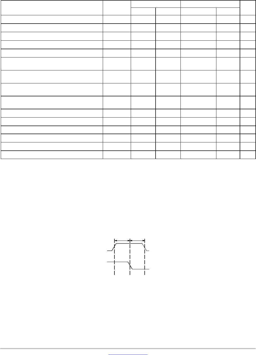
Table 20. TWO−WIRE SERIAL BUS CHARACTERISTICS (VPWR = 3.3V +0.3V; T
A
= Ambient = 25°C)
Parameter
Symbol
Standard−Mode Fast−Mode
Unit
Min Max Min Max
S
CLK
Clock Frequency
fSCL
0 100 0 400 kHz
After this period, the first clock pulse is generated
tHD;STA
4.0 − 0.6 −
s
LOW period of the S
CLK
clock
tLOW
4.7 −
1.3
−
s
HIGH period of the S
CLK
clock
tHIGH
4.0 − 0.6 −
s
Set-up time for a repeated START condition
tSU;STA
4.7 − 0.6 −
s
Data hold time
tHD;DAT
0
(Note 11)
3.45
(Note 12)
0
(Note 13)
0.9
(Note 12)
s
Data set-up time
tSU;DAT
250 −
100
(Note 13)
− ns
Rise time of both S
DATA
and S
CLK
signals t
r
−
1000
20 + 0.1Cb
(Note 14)
300 ns
Fall time of both S
DATA
and S
CLK
signals t
f
− 300
20 + 0.1Cb
(Note 14)
300 ns
Set-up time for STOP condition
tSU;STO
4.0 − 0.6 −
s
Bus free time between a STOP and START condition
tBUF
4.7 − 1.3 −
s
Capacitive load for each bus line Cb − 400 − 400 pF
Serial interface input pin capacitance
CIN_SI
− 3.3 − 3.3 pF
S
DATA
max load capacitance
CLOAD_SD
− 30 − 30 pF
S
DATA
pull−up resistor RSD 1.5 4.7 1.5 4.7
k
8. This table is based on I
2
C standard (v2.1 January 2000). Philips Semiconductor.
9. Two-wire control is I
2
C-compatible.
10.All values referred to V
IHmin
= 0.9 V
DD
and V
ILmax
= 0.1V
DD
levels. Sensor EXCLK = 27 MHz.
11. A device must internally provide a hold time of at least 300 ns for the S
DATA
signal to bridge the undefined region of the falling edge of S
CLK
.
12.The maximum t
HD;DAT
has only to be met if the device does not stretch the LOW period (t
LOW
) of the S
CLK
signal.
13.A Fast-mode I
2
C-bus device can be used in a Standard-mode I
2
C−bus system, but the requirement t
SU;DAT
250 ns must then be met. This
will automatically be the case if the device does not stretch the LOW period of the S
CLK
signal. If such a device does stretch the LOW period
of the S
CLK
signal, it must output the next data bit to the S
DATA
line t
r
max
+ t
SU;DAT
= 1000 + 250 = 1250 ns (according to the Standard−mode
I
2
C−bus specification) before the S
CLK
line is released.
14. Cb = total capacitance of one bus line in pF.
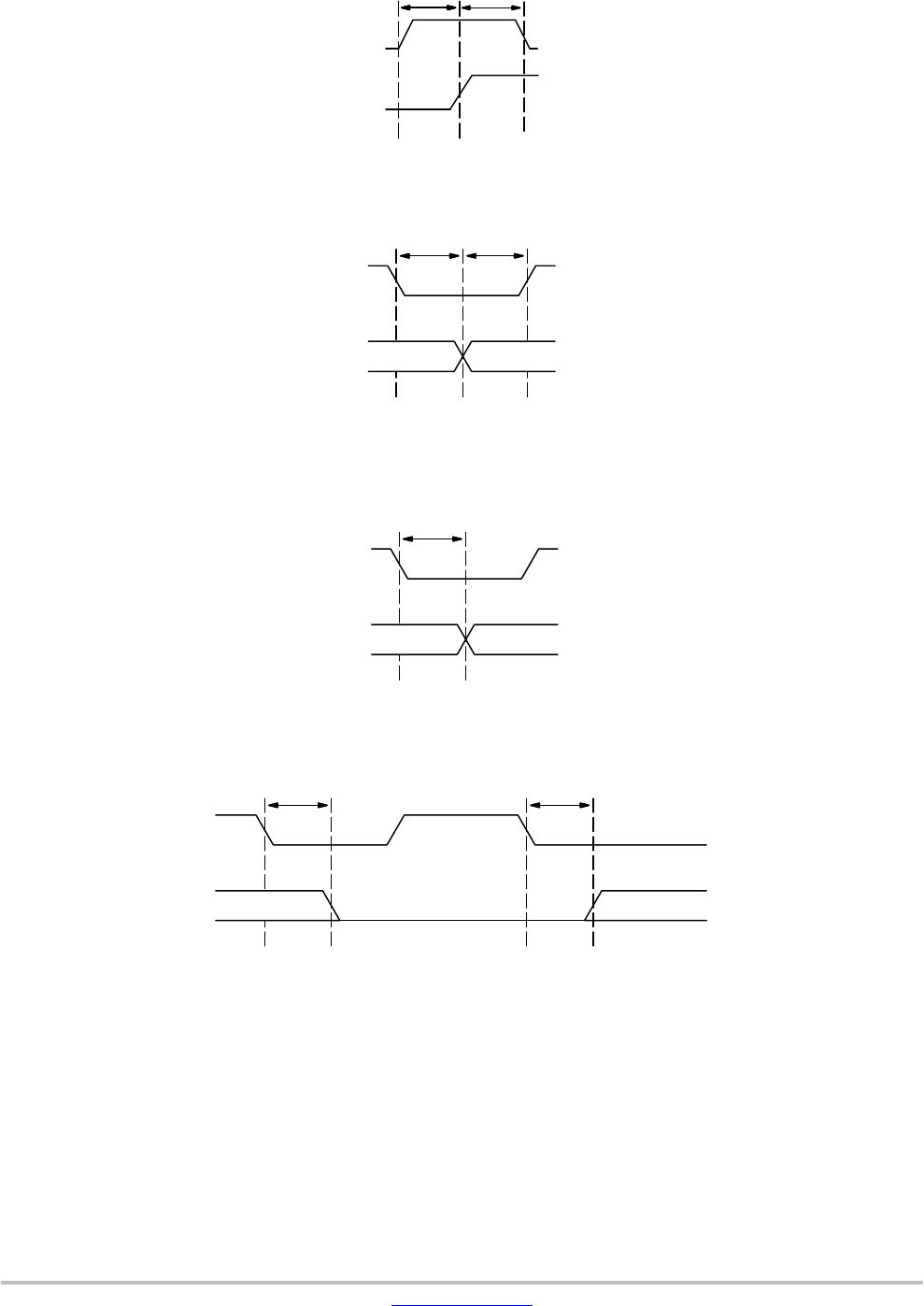
Minimum Master Clock Cycles
In addition to the AC timing requirements described in
Table 17, the two−wire serial bus operation also requires
certain minimum master clock cycles between transitions.
These are specified in Figures 41 through 46, in units of
master clock cycles.
Figure 41. Serial Host Interface Start Condition Timing
SCLK
S
DATA
44