MT9V024/D
www.onsemi.com
17
The values programmed in the window height and width
registers are the exact window height and width out of the
sensor. The window start value should never be set below
four.
To read out the dark rows set bit 6 of R0x0D. In addition,
bit 7 of R0x0D can be used to display the dark columns in
the image. Note that there are Show Dark settings only for
context A.
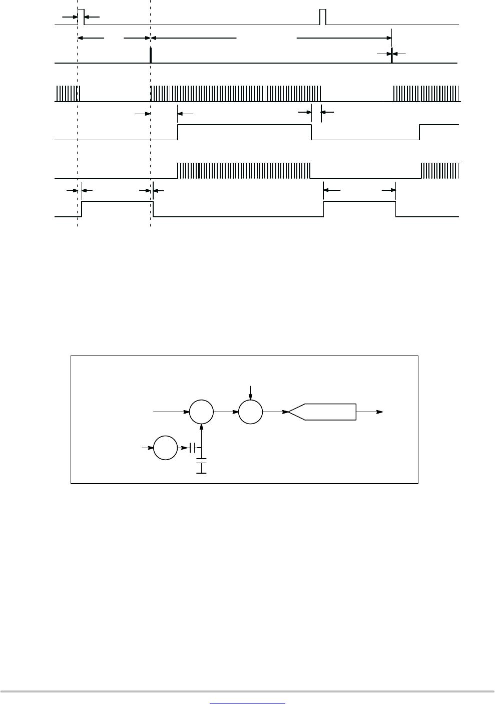
BLANKING CONTROL
Horizontal blank and vertical blank registers R0x05 and
R0x06 (B: 0xCD and R0xCE), respectively, control the
blanking time in a row (horizontal blanking) and between
frames (vertical blanking).
• Horizontal blanking is specified in terms of pixel
clocks.
• Vertical blanking is specified in terms of numbers of
rows.
The actual imager timing can be calculated using Table 2
and Table 3, which describe “Row Timing and FV/LV
signals.” The minimum number of vertical blank rows is 4.
PIXEL INTEGRATION CONTROL
Total Integration
Total integration time is the result of coarse shutter width
and fine shutter width registers, and depends also on whether
manual or automatic exposure is selected.
The actual total integration time, t
INT
is defined as:
t
INT
+ t
INTCoarse
) t
INTint
(eq. 1)
= (number of rows of integration × row time)
+ (number of pixels of integration × pixel time)
where:
• Number of Rows of Integration
(Auto Exposure Control: Enabled)
When automatic exposure control (AEC) is enabled, the
number of rows of integration may vary from frame to
frame, with the limits controlled by R0xAC (minimum
coarse shutter width) and R0xAD (maximum coarse
shutter width).
• Number of Rows of Integration
(Auto Exposure Control: Disabled)
If AEC is disabled, the number of rows of integration
equals the value in R0x0B. or
If context B is enabled, the number of rows of integration
equals the value in R0xD2.
• Number of pixels of Integration
The number of fine shutter width pixels is independent
of AEC mode (enabled or disabled):
♦ Context A: the number of pixels of integration
equals the values in R0xD5.
♦ Context B: the number of pixels of integration
equals the value in R0xD8.
Row Timing
Context A:
Row time + (R0x04 ) R0x05)master clock periods
(eq. 2)
Context B:
Row time + (R0xCC ) R0xCD) master clock periods
(eq. 3)
Typically, the value of the Coarse Shutter Width Total
registers is limited to the number of rows per frame (which
includes vertical blanking rows), such that the frame rate is
not affected by the integration time. If the Coarse Shutter
Width Total is increased beyond the total number of rows per
frame, the user must add additional blanking rows using the
Vertical Blanking registers as needed. See descriptions of
the Vertical Blanking registers, R0x06 and R0xCE in
Table 1and Table 2 of the MT9V024 register reference.
A second constraint is that
t
INT must be adjusted to avoid
banding in the image from light flicker. Under 60Hz flicker,
this means the frame time must be a multiple of 1/120 of
a second. Under 50Hz flicker, the frame time must be
a multiple of 1/100 of a second.
Changes to Integration Time
With automatic exposure control disabled (R0xAF[0] for
context A, or R0xAF[8] for context B) and if the total
integration time (R0x0B or R0xD2) is changed through the
two−wire serial interface while FV is asserted for frame n,
the first frame output using the new integration time is frame
(n + 2). Similarly, when automatic exposure control is
enabled, any change to the integration time for frame n first
appears in frame (n + 2) output. Additional details on this
latency can be found in AND9251/D − Latency of Exposure
or Gain Switch.