MT9V024/D
www.onsemi.com
22
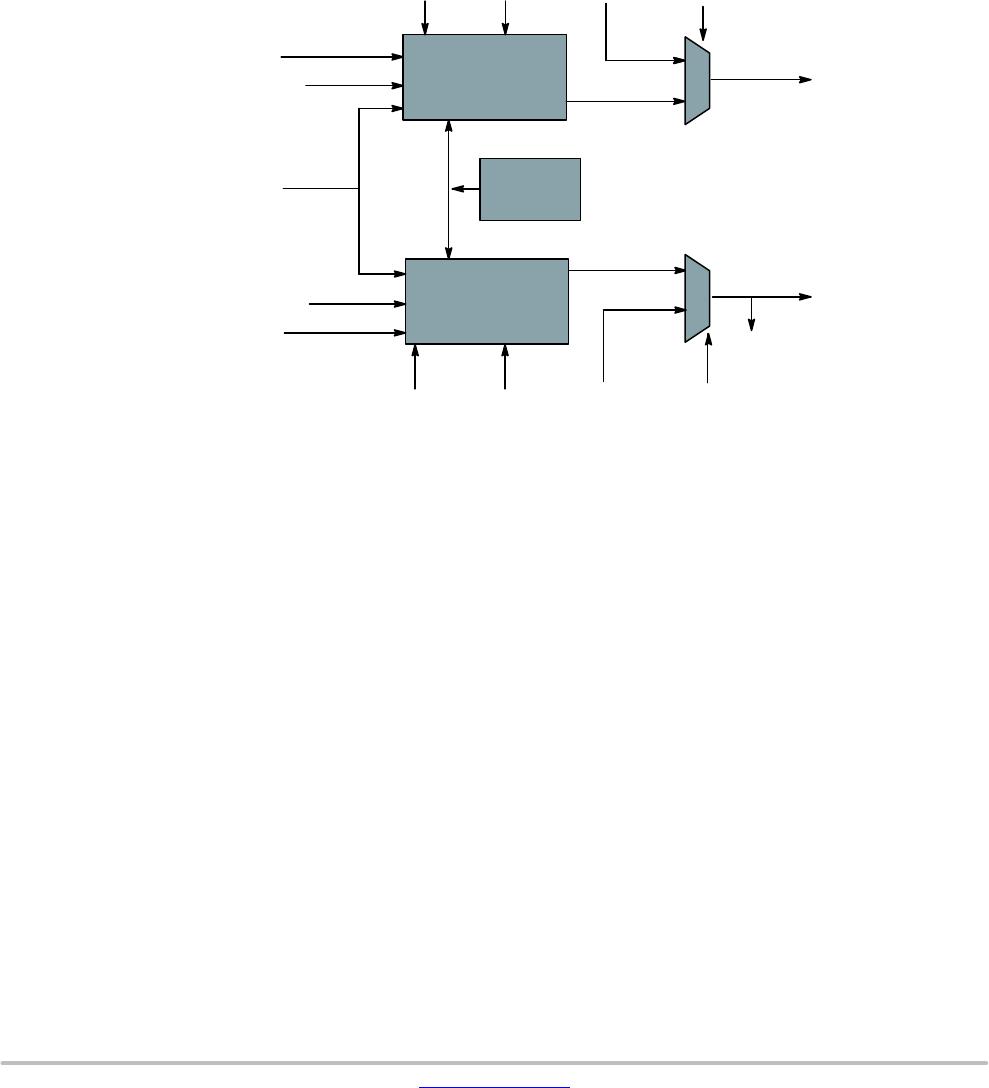
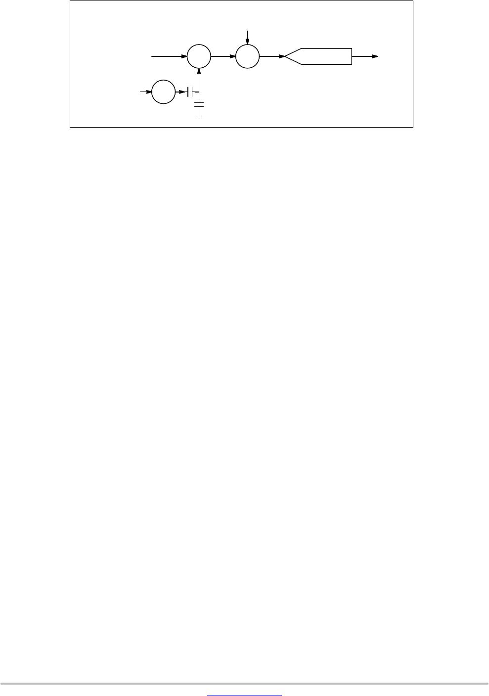
Figure 28. Black Level Calibration Flow Chart
Pixel Output
(reset minus signal)
Offset Correction
Voltage (R0x48 or
result of BLC)
Gain Selection
(R0x35 or R0x36 or
result of AGC)
ADC Data
(9:0)
10 (12) bit ADC
C1
C2
+
Σ
×
V
REF
(R0x2C)
The automatic black level calibration measures the
average value of pixels from 2 dark rows (1 dark row if row
bin 4 is enabled) of the chip. (The pixels are averaged as if
they were lightsensitive and passed through the appropriate
gain.)
This row average is then digitally lowpass filtered over
many frames (R0x47, bits 7:5) to remove temporal noise and
random instabilities associated with this measurement.
Then, the new filtered average is compared to a minimum
acceptable level, low threshold, and a maximum acceptable
level, high threshold.
If the average is lower than the minimum acceptable level,
the offset correction voltage is increased by a programmable
offset LSB in R0x4C. (Default step size is 2 LSB Offset =
1 ADC LSB at analog gain = 1X.)
If it is above the maximum level, the offset correction
voltage is decreased by 2 LSB (default).
To avoid oscillation of the black level from below to
above, the region the thresholds should be programmed so
the difference is at least two times the offset DAC step size.
In normal operation, the black level calibration
value/offset correction value is calculated at the beginning
of each frame and can be read through the twowire serial
interface from R0x48. This register is an 8bit signed twos
complement value.
However, if R0x47, bit 0 is set to “1,the calibration value
in R0x48 is used rather than the automatic black level
calculation result. This feature can be used in conjunction
with the “show dark rows” feature (R0x0D[6]) if using an
external black level calibration circuit.
The offset correction voltage is generated according to the
following formulas:
OffsetCorrectionVoltage + (8 * bit signed twoȀs complement calibration value, 127 0.25mV
(eq. 18)
ADC input voltage + (Pixel Output Voltage) * Analog Gain ) Offset Correction Voltage (AnalogGain ) 1)
(eq. 19)
Defective Pixel Correction
Defective pixel correction is intended to compensate for
defective pixels by replacing their value with a value based
on the surrounding pixels, making the defect less notice
able to the human eye. The locations of defective pixels are
stored in a ROM on chip during the manufacturing process;
the maximum number of defects stored is 32. There is no
provision for later augmenting the table of programmed
defects. In the defect correction block, bad pixels will be
substituted by either the average of its neighboring pixels, or
its nearestneighbor pixel, depending on pixel location.
Defective Pixel Correction is enabled by R0x07[9]. By
default, correction is enabled, and pixels mapped in internal
ROM are replaced with corrected values. This might be
unacceptable to some applications, in which case pixel
correction should be disabled (R0x07[9] = 0).
For complete details on using Defective Pixel Correction,
refer to AND9554/D, “Defective Pixel Correction
Description and Usage”.
Rowwise Noise Correction
Rowwise noise correction is controlled by the following
registers:
R0x70 Row Noise Control
R0x72 Row Noise Constant
Rowwise noise cancellation is performed by calculating
a row average from a set of optically black pixels at the start
of each row and then applying each average to all the active
pixels of the row. Read Dark Columns register bit and Row
Noise Correction Enable register bit must both be set to
enable rowwise noise cancellation to be performed. The
behavior when Read Dark Columns register bit = 0 and Row
Noise Correction Enable register bit = 1 is undefined.
The algorithm works as follows:
Logical columns 755790 in the pixel array provide 36
optically black pixel values. Of the 36 values, two smallest
value and two largest values are discarded. The remaining
32 values are averaged by summing them and discarding the
MT9V024/D
www.onsemi.com
23
5 LSB of the result. The 10bit result is subtracted from each
pixel value on the row in turn. In addition, a positive constant
will be added (Reg0x71, bits 7:0). This constant should be
set to the dark level targeted by the black level algorithm plus
the noise expected on the measurements of the averaged
values from dark columns; it is meant to prevent clipping
from negative noise fluctuations.
Pixel value + ADC value * dark column average ) R0x71[9 : 0]
(eq. 20)
Note that this algorithm does not work in color sensor.
Automatic Gain Control and Automatic Exposure
Control
The integrated AEC/AGC unit is responsible for ensuring
that optimal auto settings of exposure and (analog) gain are
computed and updated every frame.
AEC and AGC can be individually enabled or disabled by
R0xAF. When AEC is disabled (R0xAF[0] = 0), the sensor
uses the manual exposure value in coarse and fine shutter
width registers. When AGC is disabled (R0xAF[1] = 0), the
sensor uses the manual gain value in R0x35 or R0x36. See
“Pixel Integration Control” for more information.
MAX. EXPOSURE
(R6xBD)
DESIRED BIN
(desired luminance)
(R0xA5)
MAX. GAIN
(R0x36)
EXP. LPF
(R6xA8)
EXP. SKIP
(R0xA6)
MANUAL EXP.
(R0x08)
AEC ENABLE
(R0Xaf[0])
To exposure
timing control
To analog
gain control
R0xBA
AEC
OUTPUT
R0xBB
AGC OUTPUT
MIN GAIN
MIN EXP
GAIN LPF
(R0xAB)
GAIN SKIP
(R0xA9)
MANUAL GAIN
(R0x35)
AGC ENABLE
(R0xAF
[1])
CURRENT BIN
(current luminance
(R0xBC)
AEC
UNIT
HISTOGRAM
GENERATOR
UNIT
AGC
UNIT
1
16
Figure 29. Controllable and Observable AEC/AGC Registers
0
1
1
0
The exposure is measured in rowtime by reading
R0xBB. The exposure range is 1 to 2047. The gain is
measured in gainunits by reading R0xBA. The gain range
is 16 to 63 (unity gain = 16 gainunits; multiply by 1/16 to
get the true gain).
When AEC is enabled (R0xAF), the maximum auto
exposure value is limited by R0xBD; minimum auto
exposure is limited by AEC Minimum Exposure, R0xAC.
NOTE: AEC does not support subrow timing;
calculated exposure values are rounded down to
the nearest rowtime. For smoother response,
manual control is recommended for short
exposure times.
When AGC is enabled (R0xAF), the maximum auto gain
value is limited by R0xAB; minimum auto gain is fixed to
16 gainunits.
The exposure control measures current scene luminosity
and desired output luminosity by accumulating a histogram
of pixel values while reading out a frame. All pixels are used,
whether in color or mono mode. The desired exposure and
gain are then calculated from this for subsequent frame.
When binning is enabled, tuning of the AEC may be
required. The histogram pixel count register, R0xB0, may be
adjusted to reflect reduced pixel count. Desired bin register,
R0xA5, may be adjusted as required.
Pixel Clock Speed
The pixel clock speed is same as the master clock
(SYSCLK) at 26.66 MHz by default. However, when
column binning 2 or 4 (R0x0D or R0x0E, bit 2 or 3) is
enabled, the pixel clock speed is reduced by half and
onefourth of the master clock speed respectively. See
“Read Mode Options” and “Column Binning” for additional
information.
Hard Reset of Logic
The RC circuit for the MT9V024 uses a 10 k resistor and
a 0.1 F capacitor. The rise time for the RC circuit is 1 s
maximum.
Soft Reset of Logic
Soft reset of logic is controlled by:
R0x0C Reset
MT9V024/D
www.onsemi.com
24
Bit 0 is used to reset the digital logic of the sensor while
preserving the existing twowire serial interface
configuration. Furthermore, by asserting the soft reset, the
sensor aborts the current frame it is processing and starts
a new frame. Bit 1 is a shadowed reset control register bit to
explicitly reset the automatic gain and exposure control
feature.
These two bits are selfresetting bits and also return to “0”
during twowire serial interface reads.
STANDBY Control
The sensor goes into standby mode by setting STANDBY
to HIGH. Once the sensor detects that STANDBY is
asserted, it completes the current frame before disabling the
digital logic, internal clocks, and analog power enable
signal. To release the sensor out from the standby mode,
reset STANDBY back to LOW. The LVDS must be powered
to ensure that the device is in standby mode. See ”Appendix
A: PowerOn Reset and Standby Timing” for more
information on standby.
Monitor Mode Control
Monitor mode is controlled by:
R0xD9 Monitor Mode Enable
R0xC0 Monitor Mode Image Capture Control
The sensor goes into monitor mode when R0xD9[0] is set
to HIGH. In this mode, the sensor first captures
a programmable number of frames (R0xC0), then goes into
a sleep period for five minutes. The cycle of sleeping for five
minutes and waking up to capture a number of frames
continues until R0xD9[0] is cleared to return to normal
operation.
In some applications when monitor mode is enabled, the
purpose of capturing frames is to calibrate the gain and
exposure of the scene using automatic gain and exposure
control feature. This feature typically takes less than 10
frames to settle. In case a larger number of frames is needed,
the value of R0xC0 may be increased to capture more
frames.
During the sleep period, none of the analog circuitry and
a very small fraction of digital logic (including
a fiveminute timer) is powered. The master clock
(SYSCLK) is therefore always required.
READ MODE OPTIONS
(Also see “Output Data Format” and “Output Data
Timing”.)
Column Flip
By setting bit 5 of R0x0D or R0x0E the readout order of
the columns is reversed, as shown in Figure 30.
Row Flip
By setting bit 4 of R0x0D or R0x0E the readout order of
the rows is reversed, as shown in Figure 31.
Figure 30. Readout of Six Pixels in Normal and Column Flip Output Mode
LINE_VALID
Normal readout
D
OUT
(9:0
)
Reverse readout
D
OUT
(9:0
)
P4,1
(9:0)
P4,2
(9:0)
P4,3
(9:0)
P4,4
(9:0)
P4,5
(9:0)
P4,6
(9:0)
P4,n
(9:0)
P4,n1
(9:0)
P4,n2
(9:0)
P4,n3
(9:0)
P4,n4
(9:0)
P4,n5
(9:0)
D
OUT
(9:0)
D
OUT
(9:0)
Figure 31. Readout of Six Rows in Normal and Row Flip Output Mode
FRAME_VALID
Normal readout
D
OUT
(9:0
)
Reverse readout
D
OUT
(9:0
)
Row4
(9:0)
Row5
(9:0)
Row6
(9:0)
Row7
(9:0)
Row8
7(9:0)
Row9
(9:0)
Row484
(9:0)
Row483
(9:0)
Row482
(9:0)
Row481
(9:0)
Row480
7(9:0)
Row479
(9:0)
D
OUT
(9:0)
D
OUT
(9:0)
Pixel Binning
In addition to windowing mode in which smaller
resolutions (CIF, QCIF) are obtained by selecting a smaller
window from the sensor array, the MT9V024 also provides
the ability to downsample the entire image captured by the
pixel array using pixel binning.

MT9V024IA7XTM-DP2

Mfr. #:
Manufacturer:
ON Semiconductor
Description:
Image Sensors VGA 1/3 GS CIS Image Sensor
Lifecycle:
New from this manufacturer.
Delivery:
DHL FedEx Ups TNT EMS
Payment:
T/T Paypal Visa MoneyGram Western Union