MT9V024/D
www.onsemi.com
13
Recommended Register Settings
Table 8 describes new suggested register settings, and
descriptions of performance improvements and conditions:
Table 8. RECOMMENDED REGISTER SETTINGS AND PERFORMANCE IMPACT
(RESERVED REGISTERS)
Register Current Default New Setting Performance Impact
R0x20 0x01C1 0x03C7 Recommended by design to improve performance in HDR
mode and when frame rate is low. We also recommended
using R0x13 = 0x2D2E with this setting for better column
FPN. NOTE: When coarse integration time set to 0 and fine
integration time less than 456, R0x20 should be set to
0x01C7
R0x24 0x0010 0x001B Corrects pixel negative dark offset when global reset in
R0x20[9] is enabled.
R0x2B 0x0004 0x0003 Improves column FPN.
R0x2F 0x0004 0x0003 Improves FPN at near−saturation.
FEATURE DESCRIPTION
Operational Modes
The MT9V024 works in master, snapshot, or slave mode.
In master mode the sensor generates the readout timing. In
snapshot mode it accepts an external trigger to start
integration, then generates the readout timing. In slave mode
the sensor accepts both external integration and readout
controls. The integration time is programmed through the
two−wire serial interface during master or snapshot modes,
or controlled through an externally generated control signal
during slave mode.
Master Mode
There are two possible operation methods for master
mode: simultaneous and sequential. One of these operation
modes must be selected through the two−wire serial
inter−face. Additional details on this mode can be found in
AND9255/D Master Exposure Mode Operation.
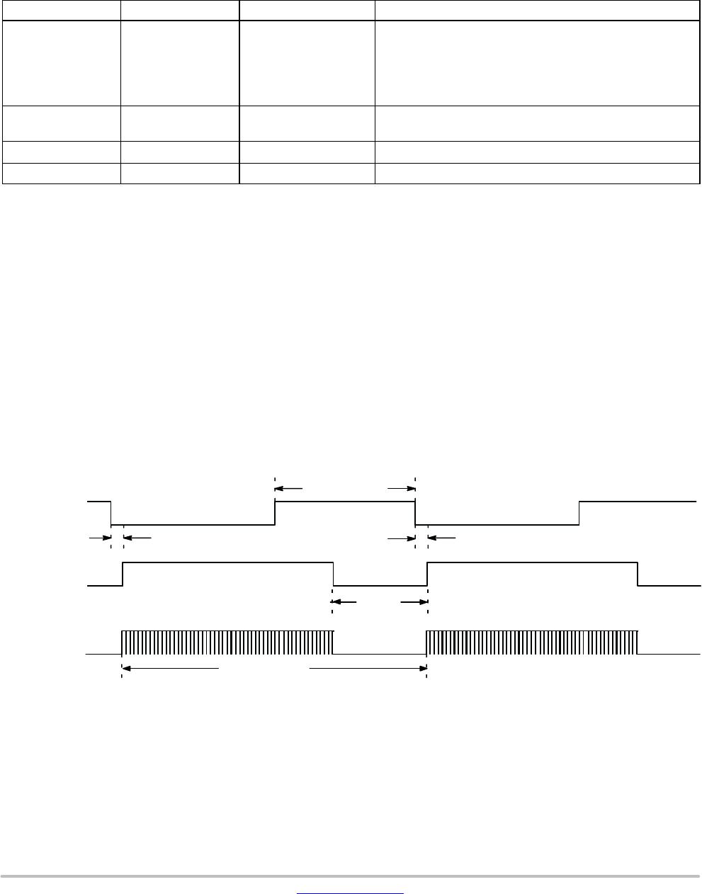
Simultaneous Master Mode
In simultaneous master mode, the exposure period occurs
during readout. The frame synchronization waveforms are
shown in Figure 14 and Figure 15. The exposure and readout
happen in parallel rather than sequential, making this the
fastest mode of operation.
EXPOSURE TIME
FRAME TIME
t
VBLANK
t
LED2FV−SIM
t
LED2FV−SIM
LED_OUT
FRAME_VALID
LINE_VALID
Figure 14. Simultaneous Master Mode Synchronization Waveforms #1

