MT9V024/D
www.onsemi.com
32
Table 18. ABSOLUTE MAXIMUM RATINGS
Symbol Parameter Minimum Maximum Unit
VSUPPLY Power supply voltage (all supplies) –0.3 4.5 V
ISUPPLY Total power supply current – 200 mA
IGND Total ground current –
200
mA
VIN DC input voltage –0.3
VDD + 0.3
V
VOUT DC output voltage –0.3
VDD + 0.3
V
TSTG (Note 7)
Storage temperature –50 +150 °C
Stresses exceeding those listed in the Maximum Ratings table may damage the device. If any of these limits are exceeded, device functionality
should not be assumed, damage may occur and reliability may be affected.
7. This is a stress rating only, and functional operation of the device at these other conditions above those indicated in the operational sections
of this specification is not implied.
Exposure to absolute maximum rating conditions for extended periods may affect reliability.
Table 19. AC ELECTRICAL CHARACTERISTICS (V
PWR
= 3.3 V ± 0.3 V; T
J
= −40°C to + 105°C; Output Load = 10pF)
Symbol Definition Condition Minimum Typical Maximum Unit
SYSCLK Input Clock Frequency 13.0 26.6 27.0 MHz
Clock Duty Cycle 45.0
50.0
55.0 %
t
R
Input Clock Rise Time – 3 5 ns
t
F
Input Clock Fall Time – 3 5 ns
t
PLH
P
SYSCLK to PIXCLK Propagation Delay CLOAD = 10 pF 4 6 8 ns
t
PD
PIXCLK to Valid DOUT(9:0) Propagation Delay CLOAD = 10 pF –3 0.6 3 ns
t
SD
Data Setup Time 14 16 – ns
t
HD
Data Hold Time 14 16 –
t
PFLR
PIXCLK to LV Propagation Delay CLOAD = 10 pF 5 7 9 ns
t
PFLF
PIXCLK to FV Propagation Delay CLOAD = 10 pF 5 7 9 ns
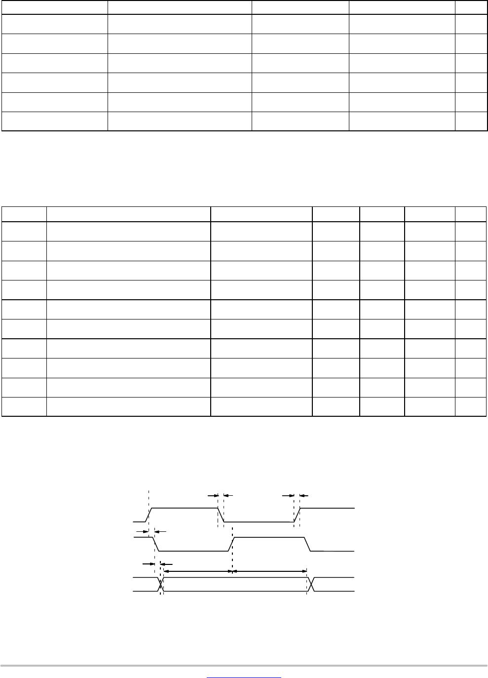
Propagation Delays for PIXCLK and Data Out Signals
The pixel clock is inverted and delayed relative to the
master clock. The relative delay from the master clock
(SYSCLK) rising edge to both the pixel clock (PIXCLK)
falling edge and the data output transition is typically 7 ns.
Note that the falling edge of the pixel clock occurs at
approximately the same time as the data output transitions.
See Table 16 for data setup and hold times.
Figure 38. Propagation Delays for PIXCLK and Data Out Signals
t
t
R
t
F
D
OUT
(9:0)
t
PLH
P
SYSCLK
PIXCLK
t
HDSD
t
PDPD
D
OUT(9:0)