MT9V024/D
www.onsemi.com
25
There are two resolution options: binning 2 and binning 4,
which reduce resolution by two or by four, respectively. Row
and column binning are separately selected. Image
mirroring options will work in conjunction with binning.
For column binning, either two or four columns are
combined by averaging to create the resulting column. For
row binning, the binning result value depends on the
difference in pixel values: for pixel signal differences of less
than 200 LSBs, the result is the average of the pixel values.
For pixel differences of greater than 200 LSBs, the result is
the value of the darker pixel value.
Row Binning
By setting bit 0 or 1 of R0x0D or R0x0E, only half or
onefourth of the row set is read out, as shown in Figure 32.
The number of rows read out is half or onefourth of the
value set in R0x03. The row binning result depends on the
difference in pixel values: for pixel signal differences less
than 200 LSBs, the result is the average of the pixel values.
For pixel differences of 200 LSBs or more, the result is the
value of the darker pixel value.
Column Binning
For column binning, either two or four columns are
combined by averaging to create the result. In setting bit 2
or 3 of R0x0D or R0x0E, the pixel data rate is slowed down
by a factor of either two or four, respectively. This is due to
the overhead time in the digital pixel data processing chain.
As a result, the pixel clock speed is also reduced accordingly.
Row10
(9:0)
Row4
(9:0)
Row5
(9:0)
Row6
(9:0)
Row7
(9:0)
Row8
7(9:0)
Row9
(9:0)
LINE_VALID
Normal readout
LINE_VALID
Row Bin 2 readout
LINE_VALID
Row Bin 4 readout
Row11
(9:0)
Row4
(9:0)
Row6
(9:0)
Row8
(9:0)
Row10
(9:0)
Row4
(9:0)
Row8
(9:0)
Figure 32. Readout of 8 Pixels in Normal and Row Bin Output Mode
D
OUT
(9:0)
D
OUT
(9:0)
D
OUT
(9:0)
Figure 33. Readout of 8 Pixels in Normal and Column Bin Output Mode
d1234
(9:0)
LINE_VALID
Normal readout
D
OUT
(9:0
)
PIXCLK
LINE_VALID
Column Bin 2 readout
D
OUT
(9:0
)
PIXCLK
LINE_VALID
Column Bin 4 readout
D
OUT
(9:0
)
PIXCLK
D1
(9:0)
D3
(9:0)
D4
(9:0)
D5
(9:0)
D6
(9:0)
D7
(9:0)
D2
(9:0)
D8
(9:0)
D12
(9:0)
D34
(9:0)
D56
(9:0)
D78
(9:0)
d5678
(9:0)
D
OUT
(9:0)
D
OUT
(9:0)
D
OUT
(9:0)
MT9V024/D
www.onsemi.com
26
Interlaced Readout
The MT9V024 has two interlaced readout options. By
setting R0x07[2:0] = 1, all the evennumbered rows are read
out first, followed by a number of programmable field
blanking rows (set by R0xBF[7:0]), then the oddnumbered
rows, and finally the vertical blanking rows. By setting
R0x07[2:0] = 2 only one field row is read out.
Consequently, the number of rows read out is half what
is set in the window height register. The row start register
determines which field gets read out; if the row start register
is even, then the even field is read out; if row start address
is odd, then the odd field is read out.
VALID IMAGE Even Field
00 00 00 ………… 00 00 00
00 00 00 ………… 00 00 00
P
4,1
P
4,2
P
4,3
…………P
4,n1
P
4,n
P
6,0
P
6,1
P
6,2
…………P
6,n1
P
6,n
00 00 00 …………………… 00 00 00
00 00 00 …………………… 00 00 00
00 00 00 ………… 00 00 00
00 00 00 ………… 00 00 00
00 00 00 ………… 00 00 00
00 00 00 ………… 00 00 00
P
m2,0
P
m2,2
………P
m2,n2
P
m2,n
P
m,2
P
m,2
…………P
m,n1
P
m,n
VALID IMAGE Odd Field
HORIZONTAL
BLANKING
FIELD BLANKING
VERTICAL BLANKING
P
5,1
P
5,2
P
5,3
…………P
5,n1
P
5,n
P
7,0
P
7,1
P
7,2
…………P
7,n1
P
7,n
P
m3,1
P
m3,2
………P
m3,n1
P
m3,n
P
m,1
P
m,1
…………P
m,n1
P
m,n
00 00 00 ……………………………… 00 00 00
00 00 00 ……………………………… 00 00 00
Figure 34. Spatial Illustration of Interlaced Image Readout
When interlaced mode is enabled, the total number of
blanking rows are determined by both field blanking register
(R0xBF) and vertical blanking register (R0x06). The
followings are their equations.
Field Blanking + R0xBF[7 : 0] (eq. 21)
Vertical Blanking + R0x06[8 : 0] * R0xBF[7 : 0] (contextA) or R0xCE[8 : 0] * R0xBF[7 : 0] (contextB) (eq. 22)
with
minimum vertical blanking requirement + 4(absolute minimum operate; see Vertical Blanking Registers
(eq. 23)
description for VBlank minimums for valid image output)
Similar to progressive scan, FV is logic LOW during the
valid image row only. Binning should not be used in
conjunction with interlaced mode.
LINE_VALID
By setting bit 2 and 3 of R0x72, the LV signal can get three
different output formats. The formats for reading out four
rows and two vertical blanking rows are shown in Figure 35.
In the last format, the LV signal is the XOR between the
continuous LV signal and the FV signal.
Default
FRAME_VALID
LINE_VALID
Continuously
FRAME_VALID
XOR
FRAME_VALID
LINE_VALID
LINE_VALID
Figure 35. Different LINE_VALID Formats
MT9V024/D
www.onsemi.com
27
LVDS Serial (StandAlone/Stereo) Output
The LVDS interface allows for the streaming of sensor
data serially to a standard offtheshelf deserializer up to
eight meters away from the sensor. The pixels (and controls)
are packeted12bit packets for standalone mode and
18bit packets for stereoscopy mode. All serial signaling
(CLK and data) is LVDS. The LVDS serial output could
either be data from a single sensor (standalone) or
streammerged data from two sensors (self and its
stereoscopic slave pair). The appendices describe in detail
the topologies for both standalone and stereoscopic modes.
There are two standard deserializers that can be used. One
for a standalone sensor stream and the other from
a stereoscopic stream. The deserializer attached to a stand
alone sensor is able to reproduce the standard parallel output
(8bit pixel data, LV, FV, and PIXCLK). The deserializer
attached to a stereoscopic sensor is able to reproduce 8 bit
pixel data from each sensor (with embedded LV and FV )
and pixelclk. An additional (simple) piece of logic is
required to extract LV and FV from the 8bit pixel data.
Irrespective of the mode (stereoscopy/standalone), LV and
FV are always embedded in the pixel data.
In stereoscopic mode, the two sensors run in lockstep,
implying all state machines are in the same state at any given
time. This is ensured by the sensorpair getting their
sysclks and sysresets in the same instance. Configuration
writes through the twowire serial interface are done in such
a way that both sensors can get their configuration updates
at once. The intersensor serial link is designed in such
a way that once the slave PLL locks and the datadly,
shftclkdly and streamlatencysel are configured, the
master sensor streams valid stereo content irrespective of
any variation voltage and/or temperature as long as it is
within specification. The configuration values of datadly,
shftclk
dly and streamlatencysel are either
predetermined from the boardlayout or can be empirically
determined by reading back the stereoerror flag. This flag
is asserted when the two sensor streams are not in sync when
merged. The combo_reg is used for outofsync diagnosis.
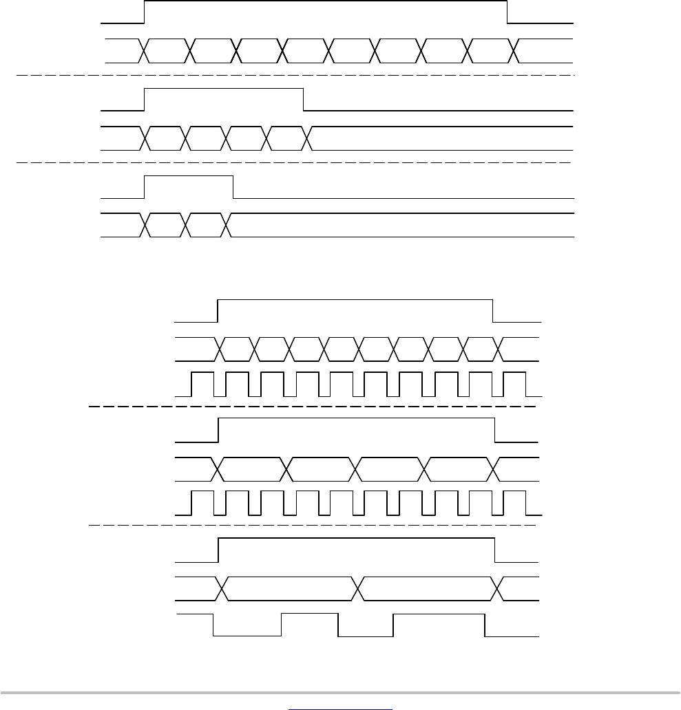
Figure 36. Serial Output Format for 6x2 Frame
Internal
PIXCLK
Internal
Parallel
Data
Internal
Line_Valid
Internal
Frame_Valid
External
Serial
Data Out
NOTES: 1. External pixel values of 0, 1, 2, 3, are reserved (they only convey control information).
Any raw pixel of value 0, 1, 2 and 3 will be substituted with 4.
2. The external pixel sequence 1023, 0 1023 is a reserved sequence (conveys control
information). Any raw pixel sequence of 1023, 0, 1023 will be substituted with 1023, 4, 1023.
P42P41 P43 P44 P45 P46 P52 P53 P54 P56
P55
P51
1023 0 1023 1 P41 P42 P43 P44 P45 P46 2 1 P51 P52 P53 P54 P55 P56 3
LVDS Output Format
In standalone mode, the packet size is 12 bits (2 frame
bits and 10 payload bits); 10bit pixels or 8bit pixels can be
selected. In 8bit pixel mode (R0xB6[0] = 0), the packet
consists of a start bit, 8bit pixel data (with sync codes), the
line valid bit, the frame valid bit and the stop bit. For 10bit
pixel mode (R0xB6[0] = 1), the packet consists of a start bit,
10bit pixel data, and the stop bit.

MT9V024IA7XTM-DP2

Mfr. #:
Manufacturer:
ON Semiconductor
Description:
Image Sensors VGA 1/3 GS CIS Image Sensor
Lifecycle:
New from this manufacturer.
Delivery:
DHL FedEx Ups TNT EMS
Payment:
T/T Paypal Visa MoneyGram Western Union