MT9V024/D
www.onsemi.com
4
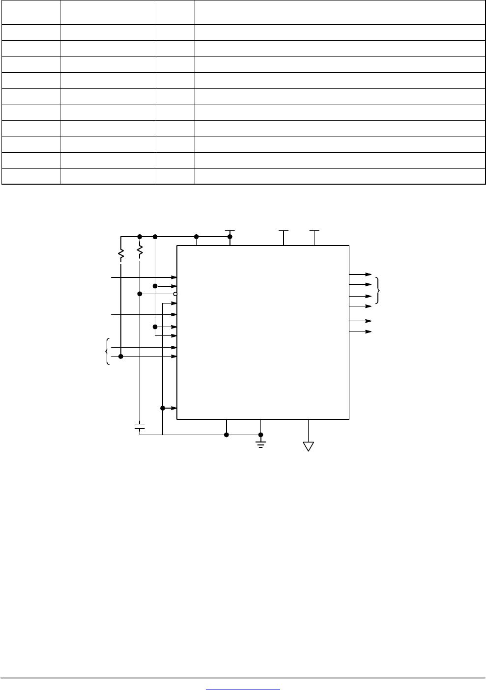
BALL DESCRIPTIONS
Table 3. BALL DESCRIPTIONS
52−Ball IBA
Numbers
Symbol Type Descriptions
H7 RSVD Input Connect to D
GND
D2 SER_DATAIN_N Input
Serial data in for stereoscopy (differential negative). Tie to 1 k pull−up (to 3.3 V)
in non−stereoscopy mode
D1 SER_DATAIN_P Input
Serial data in for stereoscopy (differential positive). Tie to D
GND
in
non−stereoscopy mode
C2 BYPASS_CLKIN_N Input
Input bypass shift−CLK (differential negative). Tie to 1 k pull−up
(to 3.3 V) in non−stereoscopy mode
C1 BYPASS_CLKIN_P Input
Input bypass shift−CLK (differential positive). Tie to D
GND
in
non−stereoscopy mode
H3 EXPOSURE Input Rising edge starts exposure in snapshot and slave modes
H4 SCLK Input
Two−wire serial interface clock. Connect to V
DD
with 1.5 k resistor even when no
other two−wire serial interface peripheral is attached
H6 OE Input D
OUT
enable pad, active HIGH
G7 S_CTRL_ADR0 Input Two−wire serial interface slave address select (see Table 4 on page 12)
H8 S_CTRL_ADR1 Input Two−wire serial interface slave address select (see Table 4 on page 12)
G8 RESET_BAR Input Asynchronous reset. All registers assume defaults
F8 STANDBY Input Shut down sensor operation for power saving
A5 SYSCLK Input Master clock (26.6 MHz; 13 MHz – 27 MHz)
G4 S
DATA
I/O
Two−wire serial interface data. Connect to V
DD
with 1.5 k resistor even when no
other two−wire serial interface peripheral is attached
G3 STLN_OUT I/O
Output in master mode−start line sync to drive slave chip in−phase; input in slave
mode
G5 STFRM_OUT I/O
Output in master mode−start frame sync to drive a slave chip in−phase; input in
slave mode
H2 LINE_VALID Output Asserted when D
OUT
data is valid
G2 FRAME_VALID Output Asserted when D
OUT
data is valid
E1 D
OUT
5 Output Parallel pixel data output 5
F1 D
OUT
6 Output Parallel pixel data output 6
F2 D
OUT
7 Output Parallel pixel data output 7
G1 D
OUT
8 Output Parallel pixel data output 8
H1 D
OUT
9 Output Parallel pixel data output 9
H5 ERROR Output Error detected. Directly connected to STEREO ERROR FLAG
G6 LED_OUT Output LED strobe output
B7 D
OUT
4 Output Parallel pixel data output 4
A8 D
OUT
3 Output Parallel pixel data output 3
A7 D
OUT
2 Output Parallel pixel data output 2
B6 D
OUT
1 Output Parallel pixel data output 1
A6 D
OUT
0 Output Parallel pixel data output 0
B5 PIXCLK Output Pixel clock out. D
OUT
is valid on rising edge of this clock
B3 SHFT_CLKOUT_N Output Output shift CLK (differential negative)
B2 SHFT_CLKOUT_P Output Output shift CLK (differential positive)