TC58NVG1S3ETAI0
2012-09-01C
31
DEVICE OPERATION
Read Mode
Read mode is set when the "00h" and “30h” commands are issued to the Command register. Between the two
commands, a start address for the Read mode needs to be issued. Refer to the figures below for the sequence and
the block diagram (Refer to the detailed timing chart.).
Random Column Address Change in Read Cycle
BY/RY
WE
CLE
RE
00h
CE
ALE
I/O
Busy
30h
Page Address N
Column Address M
M
M+1
M+2
Page Address N
t
R
Start-address input
A data transfer operation from the cell array to the Data
Cache via Page Buffer starts on the rising edge of
WE in the
30h command input cycle (after the address information has
been latched). The device will be in the Busy state during this
transfer period.
After the transfer period, the device returns to Ready state.
Serial data can be output synchronously with the
RE clock
from the start address designated in the address input cycle.
Cell array
Select page
N
M m
Data Cache
Page Buffer
I/O1 to 8: m
= 2111
Start-address input
Select page
N
M
BY/RY
WE
CLE
00h
CE
ALE
I/O
Col. M Page N
M’
Busy
Page N
30h 05h
E0h
Col. M’
M
M+1
M’ M’+1 M’+2M+3M+4
Page N
Col. M
Start from Col. M Start from Col. M’
During the serial data output from the Data Cache, the column
address can be changed by inputting a new column address
using the 05h and E0h commands. The data is read out in serial
starting at the new column address. Random Column Address
Change operation can be done multiple times within the same
page.
t
R
M+2M+3
RE
TC58NVG1S3ETAI0
2012-09-01C
32
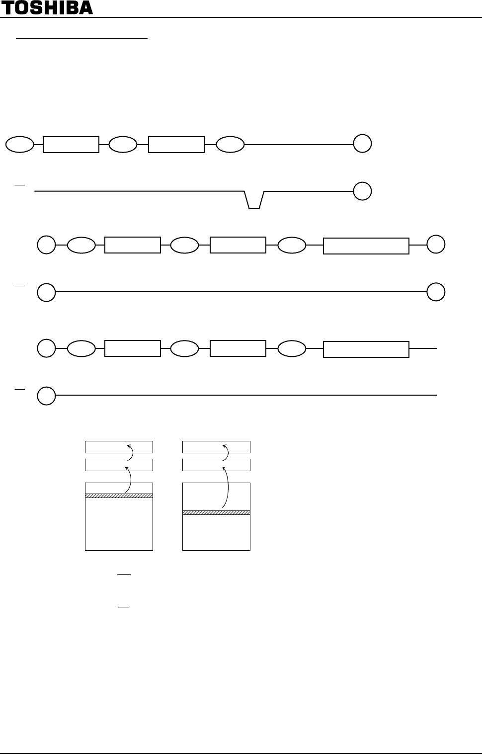
Read Operation with Read Cache
The device has a Read operation with Data Cache that enables the high speed read operation shown below. When the block address changes, this sequence has to be
started from the beginning.
Page N + 2
If the 31h command is issued to the device, the data content of the next page is transferred to the Page Buffer during serial data out from the Data Cache, and therefore the tR (Data transfer from memory
cell to data register) will be reduced.
1 Normal read. Data is transferred from Page N to Data Cache through Page Buffer. During this time period, the device outputs Busy state for tR max.
2 After the Ready/Busy returns to Ready, 31h command is issued and data is transferred to Data Cache from Page Buffer again. This data transfer takes tDCBSYR1 max and the completion of this time
period can be detected by Ready/Busy signal.
3 Data of Page N
+ 1 is transferred to Page Buffer from cell while the data of Page N in Data cache can be read out by /RE clock simultaneously.
4 The 31h command makes data of Page N
+ 1 transfer to Data Cache from Page Buffer after the completion of the transfer from cell to Page Buffer. The device outputs Busy state for tDCBSYR1 max..
This Busy period depends on the combination of the internal data transfer time from cell to Page buffer and the serial data out time.
5 Data of Page N
+ 2 is transferred to Page Buffer from cell while the data of Page N + 1 in Data cache can be read out by /RE clock simultaneously
6 The 3Fh command makes the data of Page N
+ 2 transfer to the Data Cache from the Page Buffer after the completion of the transfer from cell to Page Buffer. The device outputs Busy state for
tDCBSYR1 max.. This Busy period depends on the combination of the internal data transfer time from cell to Page buffer and the serial data out time.
7 Data of Page N
+ 2 in Data Cache can be read out, but since the 3Fh command does not transfer the data from the memory cell to Page Buffer, the device can accept new command input immediately
after the completion of serial data out.
BY/RY
WE
CLE
00h
CE
ALE
I/O
t
R
30h
Col. M Page N
0
1
23
31h 31h
0
1
23
Page Address N
Column 0
2111
Page Address N + 1
2111 0
1
23
Page Address N + 2
2111
3Fh
Data Cache
Page Buffer
Cell Array
1
2
3
3
4
5
5
1
6
7
Page N
Page N
Page N + 1
Page N
30h 31h &
RE clock
Page N + 1
Page N + 2
Page N
+ 1
31h &
RE clock
Page N + 2
3Fh & RE clock
1 2 4
3 5
6
7
t
DCBSYR1
t
DCBSYR1
t
DCBSYR1
RE
TC58NVG1S3ETAI0
2012-09-01C
33
Multi Page Read Operation
The device has a Multi Page Read operation and Multi Page Read with Data Cache operation.
(1) Multi Page Read without Data Cache
The sequence of command and address input is shown below.
Same page address (PA0 to PA5) within each district has to be selected.
The data transfer operation from the cell array to the Data Cache via Page Buffer starts on the rising
edge of
WE in the 30h command input cycle (after the 2 Districts address information has been
latched). The device will be in the Busy state during this transfer period.
After the transfer period, the device returns to Ready state. Serial data can be output synchronously
with the
RE clock from the start address designated in the address input cycle.
Selected
page
Reading
District 0 District 1
Selected
page
BY/RY
60
Command
input
Page Address
PA0 to PA16
(District 0)
tR
Address input
60
Page Address
PA0 to PA16
(District 1)
Address input
30
A
A
BY/RY
00
Command
input
Column + Page Address
CA0 to CA11, PA0 to PA16
(District 0)
Address input
05
Column Address
CA0 to CA11
(District 0)
Address input
E0
B
B
A
A
Data output
BY/RY
00
Command
input
Column + Page Address
CA0 to CA11, PA0 to PA16
(District 1)
Address input
05
Column Address
CA0 to CA11
(District 1)
Address input
E0
B
B
Data output
(District 0)
(District 1)
(3 cycle) (3 cycle)
(5 cycle)
(5 cycle)
(2 cycle)

TC58NVG1S3ETAI0

Mfr. #:
Manufacturer:
Toshiba Memory
Description:
NAND Flash 3.3V 2Gb 43nm SLC NAND (EEPROM)
Lifecycle:
New from this manufacturer.
Delivery:
DHL FedEx Ups TNT EMS
Payment:
T/T Paypal Visa MoneyGram Western Union

Products related to this Datasheet