Exar
Corporation 48720 Kato Road, Fremont CA, 94538
(510) 668-7000
FAX (510) 668-7017
www.exar.com
XR16C864
2.97V TO 5.5V QUAD UART WITH 128-BYTE FIFO
APRIL 2013 REV. 2.2.0
GENERAL DESCRIPTION
The XR16C864
1
(864) is an enhanced quad
Universal Asynchronous Receiver and Transmitter
(UART) each with 128 bytes of transmit and receive
FIFOs, transmit and receive FIFO counters and
trigger levels, automatic hardware and software flow
control, automatic RS-485 half-duplex direction
control and data rates of up to 2 Mbps. Each UART
has a set of registers that provide the user with
operating status and control, receiver error
indications, and modem serial interface controls.
System interrupts may be tailored to meet design
requirements. An internal loopback capability allows
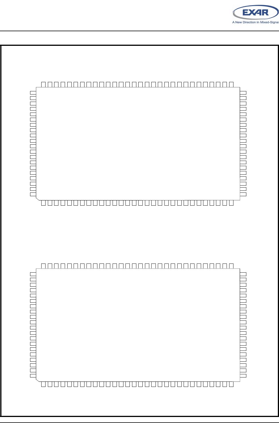
onboard diagnostics. The 864 is available in the 100-
pin QFP package. The XR16C864 offers faster
channel status access by providing separate outputs
for TXRDY and RXRDY, offer separate Infrared TX
outputs and a separate clock input for channel C
(CHCCLK). The XR16C864 is compatible with the
industry standard ST16C654 and XR16C854.
N
OTE
:
1 Covered by U.S. Patent #5,649,122 and #5,949,787.
FEATURES
Added feature in devices with top mark date code of
"F2 YYWW" and newer:
5 volt tolerant inputs
2.97 to 5.5 Volt Operation
Pin-to-pin compatible with the industry standard
ST16C654 and XR16C854
Intel or Motorola Data Bus Interface select
Four independent UART channels
Register Set Compatible to 16C550
Data rates of up to 2 Mbps
Transmit and Receive FIFOs of 128 bytes
Programmable TX and RX FIFO Trigger Levels
Transmit and Receive FIFO Level Counters
Automatic Hardware (RTS/CTS) Flow Control
Selectable Auto RTS Flow Control Hysteresis
Automatic Software (Xon/Xoff) Flow Control
Wireless Infrared (IrDA 1.0) Encoder/Decoder
Sleep Mode (200 uA typical)
Crystal oscillator or external clock input
APPLICATIONS
Portable Appliances
Telecommunication Network Routers
Ethernet Network Routers
Cellular Data Devices
Factory Automation and Process Controls
F
IGURE
1. XR16C864 B
LOCK
D
IAGRAM
X TA L1
X TA L2 C ry s tal O sc/B uffer
Intel o r
M o to ro la
D ata B us
In terface
U A R T C ha n ne l A
128 B yte T X F IFO
128 B yte R X FIF O
BR G
IR
EN D E C
TX & R X
U A R T
R egs
2.97V to 5.5V V C C
854 B LK
TX B , R X B , IR T X B, D T R B # ,
D S R B # , R TS B #, C T S B# ,
C D B# , R IB # , O P 2 B # ,
O P 1B # /R S -4 8 5
U A R T C ha n nel B
(sa m e a s C ha nnel A )
A2 :A 0
D 7:D 0
C S # A-D
16/68#
IN T A -D
IO W #
IO R #
R ese t
IN TS E L
C H C C LK
TX R D Y # A-D
R X R D Y # A -D
U A R T C ha n nel C
(sa m e a s C ha nnel A )
TX A , R X A , IR T X A, D T R A # ,
D S R A # , R TS A #, C T S A# ,
C D A# , R IA # , O P 2 A # ,
O P 1A # /R S -4 8 5
TX C , R X C , IR T X C , D TR C # ,
D S R C # , R T SC # , C TS C # ,
C D C #, R IC #, O P 2C # ,
O P 1C #/R S -485
U A R T C ha n nel D
(sa m e a s C ha nnel A )
TX D , R X D , IR T X D , D TR D # ,
D S R D # , R T SD # , C TS D # ,
C D D #, R ID #, O P 2D # ,
O P 1D #/R S -485
5V to le ran t inp uts (except XTA L1)
TC
AE N
D A C K A -D
TX D R Q # A -D
R X D R Q # A -D
D irect
M e m ory
Ac cess
BC L K A -D
C LK S E L
XR16C864
2
2.97V TO 5.5V QUAD UART WITH 128-BYTE FIFO
REV. 2.2.0
F
IGURE
2. XR16C864 P
IN
O
UT
A
SSIGNMENT
I
N
16
AND
68 M
ODE
XR16C864
100-pin QFP
16 Mode
Connect 16/68# pin to VCC
1
2
3
4
5
6
7
8
9
10
11
12
13
14
15
16
17
18
19
20
21
22
23
24
25
26
27
28
29
30
31
32
33
34
35
36
37
38
39
40
41
42
43
44
45
46
47
48
49
50
100
99
98
97
96
95
94
93
92
91
90
89
88
87
86
85
84
83
82
81
80
79
78
77
76
75
74
73
72
71
70
69
68
67
66
65
64
63
62
61
60
59
58
57
56
55
54
53
52
51
BCLKA
OP2A#
OP1A#/RS-485
DACKA
TXRDYA#/TXDRQA#
IRTXA
DSRA#
CTSA#
DTRA#
VCC
RTSA#
INTA
CSA#
TXA
IOW#
TXB
CSB#
INTB
RTSB#
GND
DTRB#
CTSB#
DSRB#
IRTXB
TXRDYB#
DACKB
AEN
OP1B#/RS-485
OP2B#
BCLKB
RXRDYB#/RXDRQB
CDB#
RIB#
RXB
CLKSEL
16/68#
A2
A1
A0
XTAL1
XTAL2
CHCCLK
RESET
RXRDY#
TXRDY#
GND
RXC
RIC#
CDC#
RXRDYC#/RXDRQC
BCLKD
OP2D#
OP1#/RS485
DACKD
FSRS#
IRTXD
DSRD#
CTSD#
DTRD#
GND
RTSD#
INTD
CSD#
TXD
IOR#
TXC
CSC#
INTC
RTSC#
VCC
DTRC#
CTSC#
DSRC#
IRTXC
TXRDYC#/TXDRQC
DACKC
TC
OP1C#/RS-485
OP2C#
BCLKC
RXRDYA#/RXDRQA
CDA#
RIA#
RXA
GND
D7
D6
D5
D4
D3
D2
D1
D0
INTSEL
VCC
RXD
RID#
CDD#
RXRDYD#/RXDRQD
TXRDYD#/TXDRQD
XR16C864
100-pin QFP
68 Mode
Connect 16/68# pin to GND
1
2
3
4
5
6
7
8
9
10
11
12
13
14
15
16
17
18
19
20
21
22
23
24
25
26
27
28
29
30
31
32
33
34
35
36
37
38
39
40
41
42
43
44
45
46
47
48
49
50
100
99
98
97
96
95
94
93
92
91
90
89
88
87
86
85
84
83
82
81
80
79
78
77
76
75
74
73
72
71
70
69
68
67
66
65
64
63
62
61
60
59
58
57
56
55
54
53
52
51
BCLKA
OP2A#
OP1A#/RS-485
DACKA
TXRDYA#/TXDRQA#
IRTXA
DSRA#
CTSA#
DTRA#
VCC
RTSA#
IRQ#
CS#
TXA
R/W#
TXB
A3
N.C.
RTSB#
GND
DTRB#
CTSB#
DSRB#
IRTXB
TXRDYB#
DACKB
AEN
OP1B#/RS-485
OP2B#
BCLKB
RXRDYB#/RXDRQB
CDB#
RIB#
RXB
CLKSEL
16/68#
A2
A1
A0
XTAL1
XTAL2
CHCCLK
RESET#
RXRDY#
TXRDY#
GND
RXC
RIC#
CDC#
RXRDYC#/RXDRQC
BCLKD
OP2D#
OP1#/RS485
DACKD
FSRS#
IRTXD
DSRD#
CTSD#
DTRD#
GND
RTSD#
N.C.
N.C.
TXD
N.C.
TXC
A4
N.C.
RTSC#
VCC
DTRC#
CTSC#
DSRC#
IRTXC
TXRDYC#/TXDRQC
DACKC
TC
OP1C#/RS-485
OP2C#
BCLKC
RXRDYA#/RXDRQA
CDA#
RIA#
RXA
GND
D7
D6
D5
D4
D3
D2
D1
D0
GND
VCC
RXD
RID#
CDD#
RXRDYD#/RXDRQD
TXRDYD#/TXDRQD
XR16C864
3
REV. 2.2.0
2.97V TO 5.5V QUAD UART WITH 128-BYTE FIFO
N
OTE
: TR = Tape and Reel, -F = Green / RoHS
PIN DESCRIPTIONS
ORDERING INFORMATION
P
ART
N
UMBER
P
ACKAGE
O
PERATING
T
EMPERATURE
R
ANGE
D
EVICE
S
TATUS
XR16C864CQ-F 100-Lead QFP C to +70°C Active
XR16C864CQTR-F 100-Lead QFP C to +70°C Active
XR16C864IQ-F 100-Lead QFP -40°C to +85°C Active
XR16C864IQTR-F 100-Lead QFP -40°C to +85°C Active
Pin Description
N
AME
100-QFP
P
IN
#
T
YPE
D
ESCRIPTION
DATA BUS INTERFACE
A2
A1
A0
37
38
39
I Address data lines [2:0]. These 3 address lines select one of the internal registers in
UART channels A-D during a data bus transaction.
D7
D6
D5
D4
D3
D2
D1
D0
95
94
93
92
91
90
89
88
I/O Data bus lines [7:0] (bidirectional).
IOR#
(N.C.)
66 I When 16/68# pin is at logic 1, the Intel bus interface is selected and this input becomes
read strobe (active low). The falling edge instigates an internal read cycle and retrieves
the data byte from an internal register pointed by the address lines [A2:A0], puts the data
byte on the data bus to allow the host processor to read it on the rising edge.
When 16/68# pin is at logic 0, the Motorola bus interface is selected and this input is not
used.
IOW#
(R/W#)
15 I When 16/68# pin is at logic 1, it selects Intel bus interface and this input becomes write
strobe (active low). The falling edge instigates the internal write cycle and the rising edge
transfers the data byte on the data bus to an internal register pointed by the address lines.
When 16/68# pin is at logic 0, the Motorola bus interface is selected and this input
becomes read (logic 1) and write (logic 0) signal.
CSA#
(CS#)
13 I When 16/68# pin is at logic 1, this input is chip select A (active low) to enable channel A in
the device.
When 16/68# pin is at logic 0, this input becomes the chip select (active low) for the
Motorola bus interface.
CSB#
(A3)
17 I When 16/68# pin is at logic 1, this input is chip select B (active low) to enable channel B in
the device.
When 16/68# pin is at logic 0, this input becomes address line A3 which is used for chan-
nel selection in the Motorola bus interface.

XR16C864IQ-F

Mfr. #:
Manufacturer:
MaxLinear
Description:
UART Interface IC UART
Lifecycle:
New from this manufacturer.
Delivery:
DHL FedEx Ups TNT EMS
Payment:
T/T Paypal Visa MoneyGram Western Union

Products related to this Datasheet