XR16C864
23
REV. 2.2.0
2.97V TO 5.5V QUAD UART WITH 128-BYTE FIFO
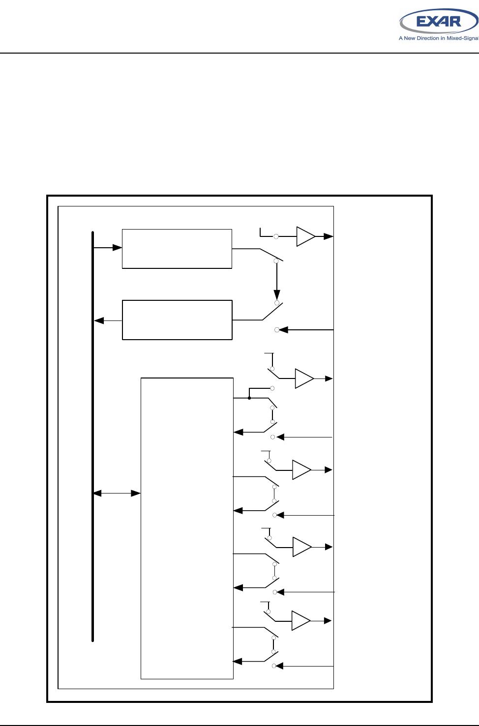
3.0 UART INTERNAL REGISTERS
Each UART channel in the 864 has its own set of configuration registers selected by address lines A0, A1 and
A2 with a specific channel selected (See
Table 1
and
Table 2
). The complete register set is shown on
Table 8
and
Table 9
.
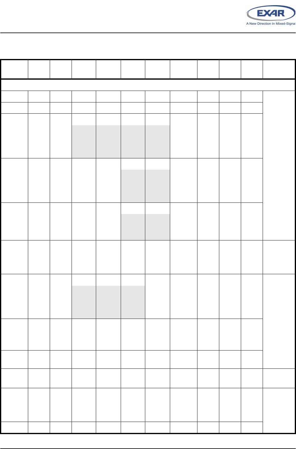
T
ABLE
8: UART INTERNAL REGISTERS
A2,A1,A0 A
DDRESSES
R
EGISTER
R
EAD
/W
RITE
C
OMMENTS
16C550 C
OMPATIBLE
R
EGISTERS
0 0 0 RHR - Receive Holding Register
THR - Transmit Holding Register
Read-only
Write-only
LCR[7] = 0
0 0 0 DLL - Div Latch Low Byte Read/Write LCR[7] = 1, LCR ≠ 0xBF
0 0 1 DLM - Div Latch High Byte Read/Write LCR[7] = 1, LCR ≠ 0xBF
0 0 0 DREV - Device Revision Code Read-only DLL, DLM = 0x00,
LCR[7] = 1, LCR ≠ 0xBF
0 0 1 DVID - Device Identification Code Read-only DLL, DLM = 0x00,
LCR[7] = 1, LCR ≠ 0xBF
0 0 1 IER - Interrupt Enable Register Read/Write LCR[7] = 0
0 1 0 ISR - Interrupt Status Register
FCR - FIFO Control Register
Read-only
Write-only
LCR[7] = 0
0 1 1 LCR - Line Control Register Read/Write
1 0 0 MCR - Modem Control Register Read/Write LCR[7] = 0
1 0 1 LSR - Line Status Register
Reserved
Read-only
Write-only
LCR[7] = 0
1 1 0 MSR - Modem Status Register
Reserved
Read-only
Write-only
LCR[7] = 0
1 1 1 SPR - Scratch Pad Register Read/Write LCR[7] = 0, FCTR[6] = 0
1 1 1 FLVL - TX/RX FIFO Level Counter Register Read-only LCR[7] = 0, FCTR[6] = 1
1 1 1 EMSR - Enhanced Mode Select Register Write-only LCR[7] = 0, FCTR[6] = 1
E
NHANCED
R
EGISTERS
0 0 0 TRG - TX/RX FIFO Trigger Level Reg
FC - TX/RX FIFO Level Counter Register
Write-only
Read-only
LCR = 0xBF
0 0 1 FCTR - Feature Control Reg Read/Write LCR = 0xBF
0 1 0 EFR - Enhanced Function Reg Read/Write LCR = 0xBF
1 0 0 Xon-1 - Xon Character 1 Read/Write LCR = 0xBF
1 0 1 Xon-2 - Xon Character 2 Read/Write LCR = 0xBF
1 1 0 Xoff-1 - Xoff Character 1 Read/Write LCR = 0xBF
1 1 1 Xoff-2 - Xoff Character 2 Read/Write LCR = 0xBF
X X X FSTAT - FIFO Status Register Read-only FSRS# pin is logic 0