XR16C864
10
2.97V TO 5.5V QUAD UART WITH 128-BYTE FIFO
REV. 2.2.0
2.2 5-Volt Tolerant Inputs
For devices that have top mark date code "F2 YYWW" and newer, the 864 can accept a voltage of up to 5.5V
on any of its inputs (except XTAL1) when operating from 2.97V to 5.5V. XTAL1 is not 5 volt tolerant. Devices
that have top mark date code "DC YYWW" and older do not have 5V tolerant inputs.
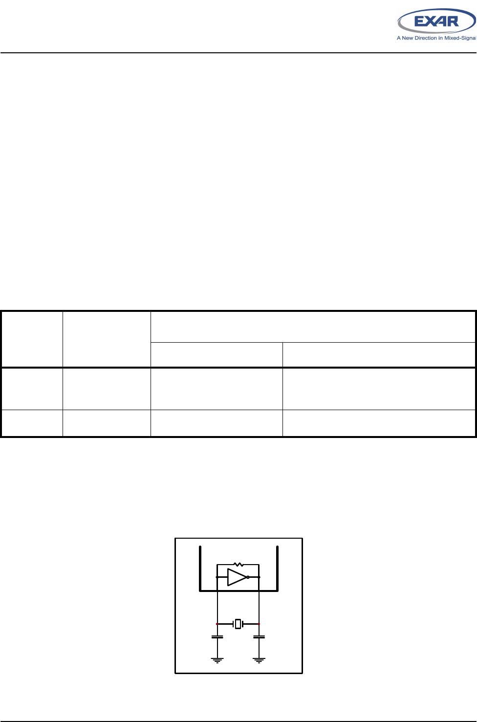
2.3 Device Reset
The RESET input resets the internal registers and the serial interface outputs in all four channels to their
default state (see Table 19). An active high pulse of longer than 40 ns duration will be required to activate the
reset function in the device. Following a power-on reset or an external reset, the 864 is software compatible
with previous generation of UARTs, 16C454 and 16C554 and 16C654.
2.4 Device Identification and Revision
The XR16C864 provides a Device Identification code and a Device Revision code to distinguish the part from
other devices and revisions. To read the identification code from the part, it is required to set the baud rate
generator registers DLL and DLM both to 0x00. Now reading the content of the DLM will provide 0x14 for the
XR16C864 and reading the content of DLL will provide the revision of the part; for example, a reading of 0x01
means revision A.
2.5 Channel Selection
The UART provides the user with the capability to bi-directionally transfer information between an external
CPU and an external serial communication device. During Intel Bus Mode (16/68# pin is connected to VCC), a
logic 0 on chip select pins, CSA#, CSB#, CSC# or CSD# allows the user to select UART channel A, B, C or D
to configure, send transmit data and/or unload receive data to/from the UART. Selecting all four UARTs can be
useful during power up initialization to write to the same internal registers, but do not attempt to read from all
four uarts simultaneously. Individual channel select functions are shown in Table 1.
During Motorola Bus Mode (16/68# pin is connected to GND), the package interface pins are configured for
connection with Motorola, and other popular microprocessor bus types. In this mode the 864 decodes two
additional addresses, A3 and A4, to select one of the four UART ports. The A3 and A4 address decode
function is used only when in the Motorola Bus Mode. See Table 2.
T
ABLE
1: C
HANNEL
A-D S
ELECT
IN
16 M
ODE
CSA# CSB# CSC# CSD# F
UNCTION
1 1 1 1 UART de-selected
0 1 1 1 Channel A selected
1 0 1 1 Channel B selected
1 1 0 1 Channel C selected
1 1 1 0 Channel D selected
0 0 0 0 Channels A-D selected
T
ABLE
2: C
HANNEL
A-D S
ELECT
IN
68 M
ODE
CS# A4 A3 F
UNCTION
1 N/A N/A UART de-selected
0 0 0 Channel A selected
0 0 1 Channel B selected
0 1 0 Channel C selected
0 1 1 Channel D selected
XR16C864
11
REV. 2.2.0
2.97V TO 5.5V QUAD UART WITH 128-BYTE FIFO
2.6 Channels A-D Internal Registers
Each UART channel in the 864 has a set of enhanced registers for control, monitoring and data loading and
unloading. The configuration register set is compatible to those already available in the standard single
16C550. These registers function as data holding registers (THR/RHR), interrupt status and control registers
(ISR/IER), a FIFO control register (FCR), receive line status and control registers (LSR/LCR), modem status
and control registers (MSR/MCR), programmable data rate (clock) divisor registers (DLL/DLM), and a user
accessible scratchpad register (SPR).
Beyond the general 16C550 features and capabilities, the 864 offers enhanced feature registers (EMSR, FLVL,
EFR, Xon/Xoff 1, Xon/Xoff 2, FCTR, TRG, FC) that provide automatic RTS and CTS hardware flow control,
Xon/Xoff software flow control, automatic RS-485 half-duplex direction output enable/disable, FIFO trigger
level control, and FIFO level counters. All the register functions are discussed in full detail later in “Section
3.0, UART Internal Registers” on page 23.
2.7 INT Ouputs for Channels A-D
The interrupt outputs change according to the operating mode and enhanced features setup. Table 3 and 4
summarize the operating behavior for the transmitter and receiver. Also see Figure 19 through 23.
T
ABLE
3: INT P
INS
O
PERATION
FOR
T
RANSMITTER
FOR
C
HANNELS
A-D
FCTR
Bit-3
FCR B
IT
-0 = 0
(FIFO D
ISABLED
)
FCR B
IT
-0 = 1 (FIFO E
NABLED
)
FCR Bit-3 = 0
(DMA Mode Disabled)
FCR Bit-3 = 1
(DMA Mode Enabled)
INT Pin 0 0 = a byte in THR
1 = THR empty
0 = FIFO above trigger level
1 = FIFO below trigger level or FIFO
empty
0 = FIFO above trigger level
1 = FIFO below trigger level or FIFO
empty
INT Pin 1 0 = a byte in THR
1 = transmitter empty
0 = FIFO above trigger level
1 = FIFO below trigger level or
transmitter empty
0 = FIFO above trigger level
1 = FIFO below trigger level or
transmitter empty
T
ABLE
4: INT P
IN
O
PERATION
FOR
R
ECEIVER
FOR
C
HANNELS
A-D
FCR B
IT
-0 = 0
(FIFO D
ISABLED
)
FCR B
IT
-0 = 1 (FIFO E
NABLED
)
FCR Bit-3 = 0
(DMA Mode Disabled)
FCR Bit-3 = 1
(DMA Mode Enabled)
INT Pin 0 = no data
1 = 1 byte
0 = FIFO below trigger level
1 = FIFO above trigger level
0 = FIFO below trigger level
1 = FIFO above trigger level
XR16C864
12
2.97V TO 5.5V QUAD UART WITH 128-BYTE FIFO
REV. 2.2.0
2.8 Direct Memory Access
In this document, Direct Memory Access will not be referred to by its acronym (DMA) to avoid confusion with
DMA Mode (a legacy term) that refers to data block transfer operation. Direct Memory Access mode is enabled
via EMSR bits 2 and 3. The Direct Memory Access transaction is controlled through the RXDRQ [A-D],
TXDRQ [A-D], DACK [A-D], AEN and TC pins.
2.9 DMA Mode
The DMA Mode (a legacy term) in this document doesn’t mean “direct memory access” but refers to data block
transfer operation. (Since the 864 also supports Direct Memory Access, “Direct Memory Access” will be used
instead of “DMA” when explaining Direct Memory Access.) The DMA mode affects the state of the RXRDY# A-
D and TXRDY# A-D output pins. The transmit and receive FIFO trigger levels provide additional flexibility to the
user for block mode operation. The LSR bits 5-6 provide an indication when the transmitter is empty or has an
empty location(s) for more data. The user can optionally operate the transmit and receive FIFO in the DMA
mode (FCR bit-3=1). When the transmit and receive FIFO are enabled and the DMA mode is disabled (FCR
bit-3 = 0), the 864 is placed in single-character mode for data transmit or receive operation. When DMA mode
is enabled (FCR bit-3 = 1), the user takes advantage of block mode operation by loading or unloading the FIFO
in a block sequence determined by the programmed trigger level. The following table show their behavior. Also
see Figure 19 through 23.
2.10 Crystal Oscillator or External Clock Input
The 864 includes an on-chip oscillator (XTAL1 and XTAL2) to produce a clock for all four UART sections in the
device. The CPU data bus does not require this clock for bus operation. The crystal oscillator provides a
system clock to the Baud Rate Generators (BRG) section found in each of the UART. XTAL1 is the input to the
oscillator or external clock buffer input with XTAL2 pin being the output. For programming details, see
“Programmable Baud Rate Generator.”
F
IGURE
4. T
YPICAL
OSCILATOR
CONNECTIONSL
The on-chip oscillator is designed to use an industry standard microprocessor crystal (parallel resonant,
fundamental frequency with 10-22 pF capacitance load, ESR of 20-120 ohms and 100ppm frequency
T
ABLE
5: TXRDY#
AND
RXRDY# O
UTPUTS
IN
FIFO
AND
DMA M
ODE
FOR
C
HANNELS
A-D
P
INS
FCR
BIT
-0=0
(FIFO D
ISABLED
)
FCR B
IT
-0=1 (FIFO E
NABLED
)
FCR Bit-3 = 0
(DMA Mode Disabled)
FCR Bit-3 = 1
(DMA Mode Enabled)
RXRDY#
0 = 1 byte
1 = no data
0 = at least 1 byte in FIFO
1 = FIFO empty
1 to 0 transition when FIFO reaches the trigger
level, or timeout occurs.
0 to 1 transition when FIFO empties.
TXRDY#
0 = THR empty
1 = byte in THR
0 = FIFO empty
1 = at least 1 byte in FIFO
0 = FIFO has at least 1 empty location.
1 = FIFO is full.
C1
22-47pF
C2
22-47pF
14.7456
M Hz
XTAL1
XTAL2
R=300K to 400K

XR16C864IQ-F

Mfr. #:
Manufacturer:
MaxLinear
Description:
UART Interface IC UART
Lifecycle:
New from this manufacturer.
Delivery:
DHL FedEx Ups TNT EMS
Payment:
T/T Paypal Visa MoneyGram Western Union

Products related to this Datasheet