XR16C864
15
REV. 2.2.0
2.97V TO 5.5V QUAD UART WITH 128-BYTE FIFO
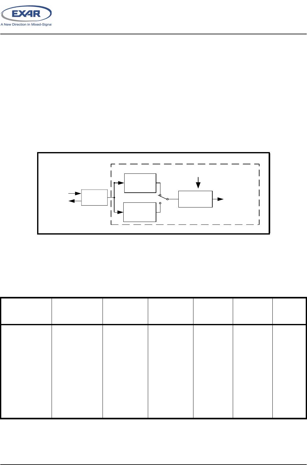
2.13 Receiver
The receiver section contains an 8-bit Receive Shift Register (RSR) and 128 bytes of FIFO which includes a
byte-wide Receive Holding Register (RHR). The RSR uses the 16X clock for timing. It verifies and validates
every bit on the incoming character in the middle of each data bit. On the falling edge of a start or false start bit,
an internal receiver counter starts counting at the 16X clock rate. After 8 clocks the start bit period should be at
the center of the start bit. At this time the start bit is sampled and if it is still a logic 0 it is validated. Evaluating
the start bit in this manner prevents the receiver from assembling a false character. The rest of the data bits
and stop bits are sampled and validated in this same manner to prevent false framing. If there were any
error(s), they are reported in the LSR register bits 2-4. Upon unloading the receive data byte from RHR, the
receive FIFO pointer is bumped and the error tags are immediately updated to reflect the status of the data
byte in RHR register. RHR can generate a receive data ready interrupt upon receiving a character or delay until
it reaches the FIFO trigger level. Furthermore, data delivery to the host is guaranteed by a receive data ready
time-out interrupt when data is not received for 4 word lengths as defined by LCR[1:0] plus 12 bits time. This is
equivalent to 3.7-4.6 character times. The RHR interrupt is enabled by IER bit-0.
2.13.1 Receive Holding Register (RHR) - Read-Only
The Receive Holding Register is an 8-bit register that holds a receive data byte from the Receive Shift
Register. It provides the receive data interface to the host processor. The RHR register is part of the receive
FIFO of 128 bytes by 11-bits wide, the 3 extra bits are for the 3 error tags to be reported in LSR register. When
the FIFO is enabled by FCR bit-0, the RHR contains the first data character received by the FIFO. After the
RHR is read, the next character byte is loaded into the RHR and the errors associated with the current data
byte are immediately updated in the LSR bits 2-4.
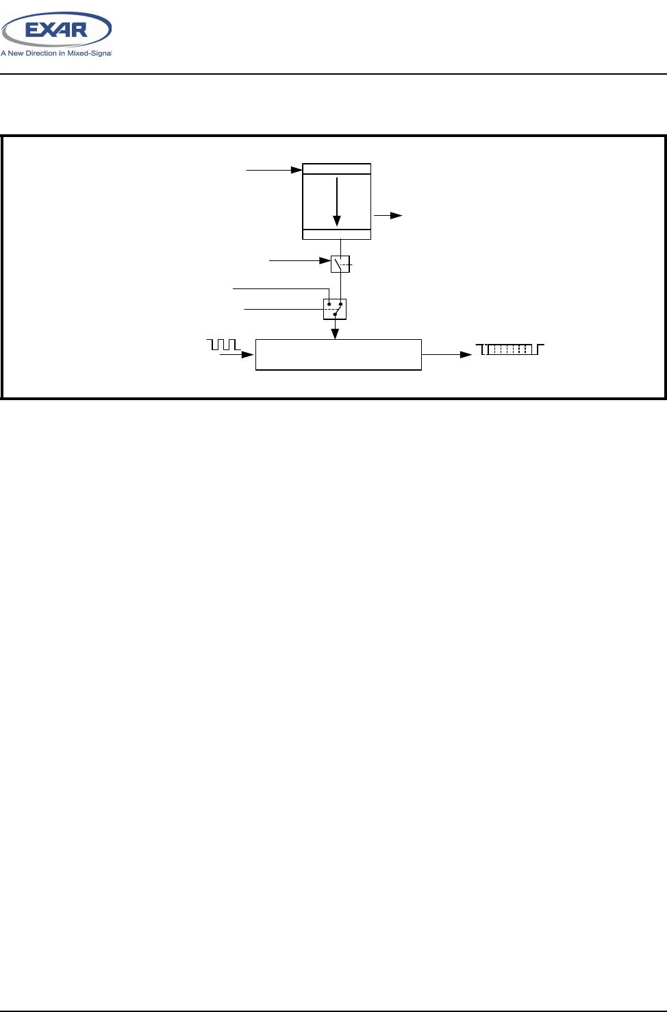
F
IGURE
7. T
RANSMITTER
O
PERATION
IN
FIFO
AND
F
LOW
C
ONTROL
M
ODE
Transmit Data Shift Register
(TSR)
Data Byte
THR Interrupt (ISR bit-1) falls
below the programmed Trigger
Level and then when becomes
empty. FIFO is Enabled by FCR
bit-0=1
RX FIFO
16X Clock
Auto CTS Flow Control (CTS# pin)
Auto Software Flow Control
Flow Control Characters
(Xoff1/2 and Xon1/2 Reg.
TXF IFO1
THR