
XR16C864
31
REV. 2.2.0
2.97V TO 5.5V QUAD UART WITH 128-BYTE FIFO
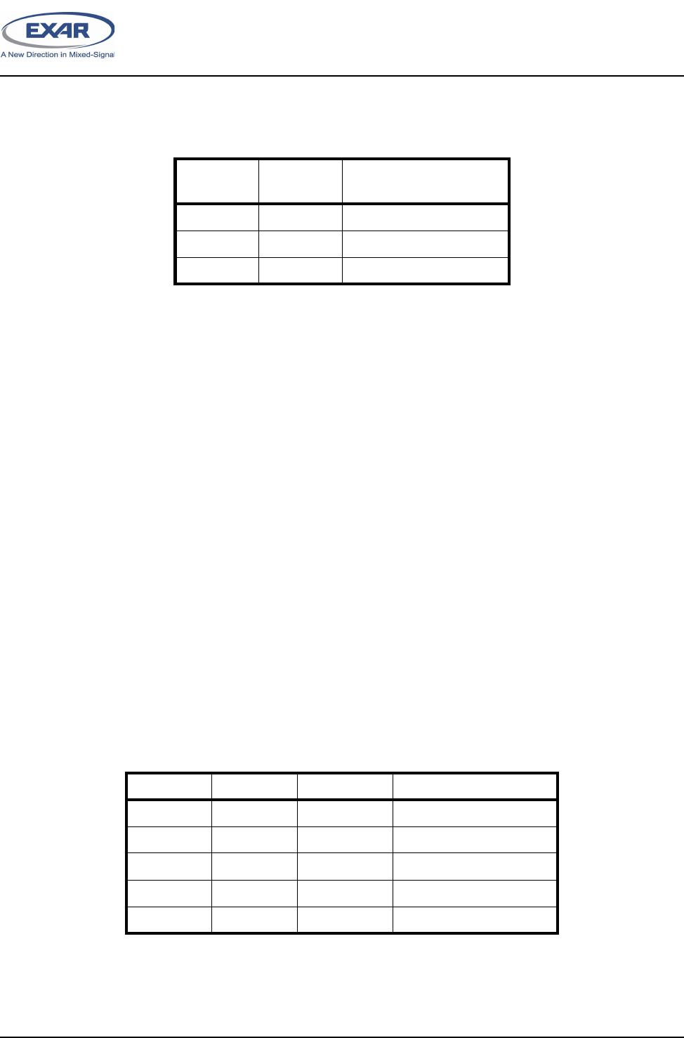
LCR[2]: TX and RX Stop-bit Length Select
The length of stop bit is specified by this bit in conjunction with the programmed word length.
LCR[3]: TX and RX Parity Select
Parity or no parity can be selected via this bit. The parity bit is a simple way used in communications for data
integrity check. See
Table 12
for parity selection summary below.
Logic 0 = No parity.
Logic 1 = A parity bit is generated during the transmission while the receiver checks for parity error of the
data character received.
LCR[4]: TX and RX Parity Select
If the parity bit is enabled with LCR bit-3 set to a logic 1, LCR BIT-4 selects the even or odd parity format.
Logic 0 = ODD Parity is generated by forcing an odd number of logic 1’s in the transmitted character. The
receiver must be programmed to check the same format (default).
Logic 1 = EVEN Parity is generated by forcing an even number of logic 1’s in the transmitted character. The
receiver must be programmed to check the same format.
LCR[5]: TX and RX Parity Select
If the parity bit is enabled, LCR BIT-5 selects the forced parity format.
LCR BIT-5 = logic 0, parity is not forced (default).
LCR BIT-5 = logic 1 and LCR BIT-4 = logic 0, parity bit is forced to a logical 1 for the transmit and receive
data.
LCR BIT-5 = logic 1 and LCR BIT-4 = logic 1, parity bit is forced to a logical 0 for the transmit and receive
data.
BIT-2
W
ORD
LENGTH
S
TOP
BIT
LENGTH
(B
IT
TIME
(
S
))
0 5,6,7,8 1 (default)
1 5 1-1/2
1 6,7,8 2
T
ABLE
12: P
ARITY
SELECTION
LCR B
IT
-5 LCR B
IT
-4 LCR B
IT
-3 P
ARITY
SELECTION
X X 0 No parity
0 0 1 Odd parity
0 1 1 Even parity
1 0 1 Force parity to mark, “1”
1 1 1 Forced parity to space, “0”
XR16C864
32
2.97V TO 5.5V QUAD UART WITH 128-BYTE FIFO
REV. 2.2.0
LCR[6]: Transmit Break Enable
When enabled, the Break control bit causes a break condition to be transmitted (the TX output is forced to a
“space’, logic 0, state). This condition remains, until disabled by setting LCR bit-6 to a logic 0.
Logic 0 = No TX break condition (default).
Logic 1 = Forces the transmitter output (TX) to a “space”, logic 0, for alerting the remote receiver of a line
break condition.
LCR[7]: Baud Rate Divisors Enable
Logic 0 = Data registers are selected (default).
Logic 1 = Divisor latch registers are selected.
4.7 Modem Control Register (MCR) or General Purpose Outputs Control - Read/Write
The MCR register is used for controlling the serial/modem interface signals or general purpose inputs/outputs.
MCR[0]: DTR# Output
The DTR# pin is a modem control output. If the modem interface is not used, this output may be used as a
general purpose output.
Logic 0 = Force DTR# output to a logic 1 (default).
Logic 1 = Force DTR# output to a logic 0.
MCR[1]: RTS# Output
The RTS# pin is a modem control output and may be used for automatic hardware flow control by enabled by
EFR bit-6. If the modem interface is not used, this output may be used as a general purpose output.
Logic 0 = Force RTS# output to a logic 1 (default).
Logic 1 = Force RTS# output to a logic 0.
MCR[2]: OP1# Output or RS485 Output Control
In the Loopback Mode, this bit is used to write the state of the modem RI# interface signal. If Auto RS-485
Half-Duplex direction control is enabled via FCTR bit-3, MCR bit-2 should not be written to.
MCR[3]: INT Output Enable
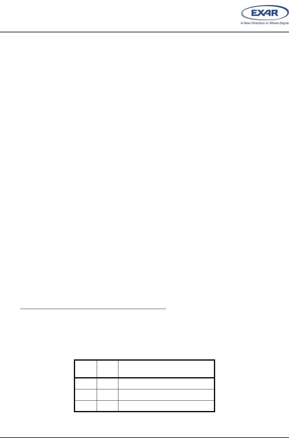
Enable or disable INT outputs to become active or in three-state. This function is associated with the INTSEL
input, see below table for details. This bit is also used to control the OP2# signal during internal loopback
mode. INTSEL pin must be set to a logic zero during 68 mode.
Logic 0 = INT (A-D) outputs disabled (three state) in the 16 mode (default). During loopback mode, it sets
OP2# internally to a logic 1.
Logic 1 = INT (A-D) outputs enabled (active) in the 16 mode. During loopback mode, it sets OP2# internally
to a logic 0.
T
ABLE
13: INT O
UTPUT
M
ODES
INTSEL
P
IN
MCR
B
IT
-3
INT A-D O
UTPUTS
IN
16 M
ODE
0 0 Three-State
0 1 Active
1 X Active
XR16C864
33
REV. 2.2.0
2.97V TO 5.5V QUAD UART WITH 128-BYTE FIFO
MCR[4]: Internal Loopback Enable
Logic 0 = Disable loopback mode (default).
Logic 1 = Enable local loopback mode, see loopback section and
Figure 12
.
MCR[5]: Xon-Any Enable
Logic 0 = Disable Xon-Any function (for 16C550 compatibility, default).
Logic 1 = Enable Xon-Any function. In this mode, any RX character received will resume transmit operation.
The RX character will be loaded into the RX FIFO , unless the RX character is an Xon or Xoff character and
the 864 is programmed to use the Xon/Xoff flow control.
MCR[6]: Infrared Encoder/Decoder Enable
Logic 0 = Enable the standard modem receive and transmit input/output interface (default).
Logic 1 = Enable infrared IrDA receive and transmit inputs/outputs. The TX/RX output/input are routed to the
infrared encoder/decoder. The data input and output levels conform to the IrDA infrared interface
requirement. The RX FIFO may need to be flushed upon enable. While in this mode, the infrared TX output
will be a logic 0 during idle data conditions.
MCR[7]: Clock Prescaler Select
The CLKSEL pin selects this function upon power up or reset. After the power up or reset, this register bit will
have control and can alter the logic state.
Logic 0 = Divide by one. The input clock from the crystal or external clock is fed directly to the Programmable
Baud Rate Generator without further modification, i.e., divide by one (default).
Logic 1 = Divide by four. The prescaler divides the input clock from the crystal or external clock by four and
feeds it to the Programmable Baud Rate Generator, hence, data rates become one forth.
4.8 Line Status Register (LSR) - Read Only
This register provides the status of data transfers between the UART and the host. If LSR bits 1-4 are
asserted, an interrupt will be generated immediately if IER bit-2 is enabled.
LSR[0]: Receive Data Ready Indicator
Logic 0 = No data in receive holding register or FIFO (default).
Logic 1 = Data has been received and is saved in the receive holding register or FIFO.
LSR[1]: Receiver Overrun Flag
Logic 0 = No overrun error (default).
Logic 1 = Overrun error. A data overrun error condition occurred in the receive shift register. This happens
when additional data arrives while the FIFO is full. In this case the previous data in the receive shift register
is overwritten. Note that under this condition the data byte in the receive shift register is not transferred into
the FIFO, therefore the data in the FIFO is not corrupted by the error.
LSR[2]: Receive Data Parity Error Tag
Logic 0 = No parity error (default).
Logic 1 = Parity error. The receive character in RHR does not have correct parity information and is suspect.
This error is associated with the character available for reading in RHR.
LSR[3]: Receive Data Framing Error Tag
Logic 0 = No framing error (default).
Logic 1 = Framing error. The receive character did not have a valid stop bit(s). This error is associated with
the character available for reading in RHR.
XR16C864IQ-F

Mfr. #:
Manufacturer:
MaxLinear
Description:
UART Interface IC UART
Lifecycle:
New from this manufacturer.
Delivery:
DHL FedEx Ups TNT EMS
Payment:
T/T Paypal Visa MoneyGram Western Union

Products related to this Datasheet