XR16C864
28
2.97V TO 5.5V QUAD UART WITH 128-BYTE FIFO
REV. 2.2.0
4.4.2 Interrupt Clearing:
LSR interrupt is cleared by a read to the LSR register.
RXRDY interrupt is cleared by reading data until FIFO falls below the trigger level.
RXRDY Time-out interrupt is cleared by reading RHR.
TXRDY interrupt is cleared by a read to the ISR register or writing to THR.
MSR interrupt is cleared by a read to the MSR register.
Xoff interrupt is cleared by a read to ISR or when Xon character(s) is received.
Special character interrupt is cleared by a read to ISR or after the next character is received.
RTS# and CTS# flow control interrupts are cleared by a read to the MSR register.
]
ISR[0]: Interrupt Status
Logic 0 = An interrupt is pending and the ISR contents may be used as a pointer to the appropriate interrupt
service routine.
Logic 1 = No interrupt pending (default condition).
ISR[3:1]: Interrupt Status
These bits indicate the source for a pending interrupt at interrupt priority levels (See Interrupt Source
Table 10
).
ISR[5:4]: Interrupt Status
These bits are enabled when EFR bit-4 is set to a logic 1. ISR bit-4 indicates that the receiver detected a data
match of the Xoff character(s). Note that once set to a logic 1, the ISR bit-4 will stay a logic 1 until a Xon
character is received. ISR bit-5 indicates that CTS# or RTS# has changed state.
ISR[7:6]: FIFO Enable Status
These bits are set to a logic 0 when the FIFOs are disabled. They are set to a logic 1 when the FIFOs are
enabled.
T
ABLE
10: I
NTERRUPT
S
OURCE
AND
P
RIORITY
L
EVEL
P
RIORITY
ISR R
EGISTER
S
TATUS
B
ITS
S
OURCE
OF
INTERRUPT
L
EVEL
B
IT
-5 B
IT
-4 B
IT
-3 B
IT
-2 B
IT
-1 B
IT
-0
1 0 0 0 1 1 0 LSR (Receiver Line Status Register)
2 0 0 1 1 0 0 RXRDY (Receive Data Time-out)
3 0 0 0 1 0 0 RXRDY (Received Data Ready)
4 0 0 0 0 1 0 TXRDY (Transmit Ready)
5 0 0 0 0 0 0 MSR (Modem Status Register)
6 0 1 0 0 0 0 RXRDY (Received Xoff or Special character)
7 1 0 0 0 0 0 CTS#, RTS# change of state
- 0 0 0 0 0 1 None (default)
XR16C864
29
REV. 2.2.0
2.97V TO 5.5V QUAD UART WITH 128-BYTE FIFO
4.5 FIFO Control Register (FCR) - Write-Only
This register is used to enable the FIFOs, clear the FIFOs, set the transmit/receive FIFO trigger levels, and
select the DMA mode. The DMA and FIFO modes are defined as follows:
FCR[0]: TX and RX FIFO Enable
Logic 0 = Disable the transmit and receive FIFO (default).
Logic 1 = Enable the transmit and receive FIFOs. This bit must be set to logic 1 when other FCR bits are
written or they will not be programmed.
FCR[1]: RX FIFO Reset
This bit is only active when FCR bit-0 is a ‘1’.
Logic 0 = No receive
FIFO
reset (default)
Logic 1 = Reset the receive FIFO pointers and FIFO level counter logic (the receive shift register is not
cleared or altered). This bit will return to a logic 0 after resetting the FIFO.
FCR[2]: TX FIFO Reset
This bit is only active when FCR bit-0 is a ‘1’.
Logic 0 = No transmit FIFO reset (default).
Logic 1 = Reset the transmit FIFO pointers and FIFO level counter logic (the transmit shift register is not
cleared or altered). This bit will return to a logic 0 after resetting the FIFO.
FCR[3]: DMA Mode Select
Controls the behavior of the TXRDY# and RXRDY# pins. See DMA operation section for details.
Logic 0 = Normal Operation (default).
Logic 1 = DMA Mode.
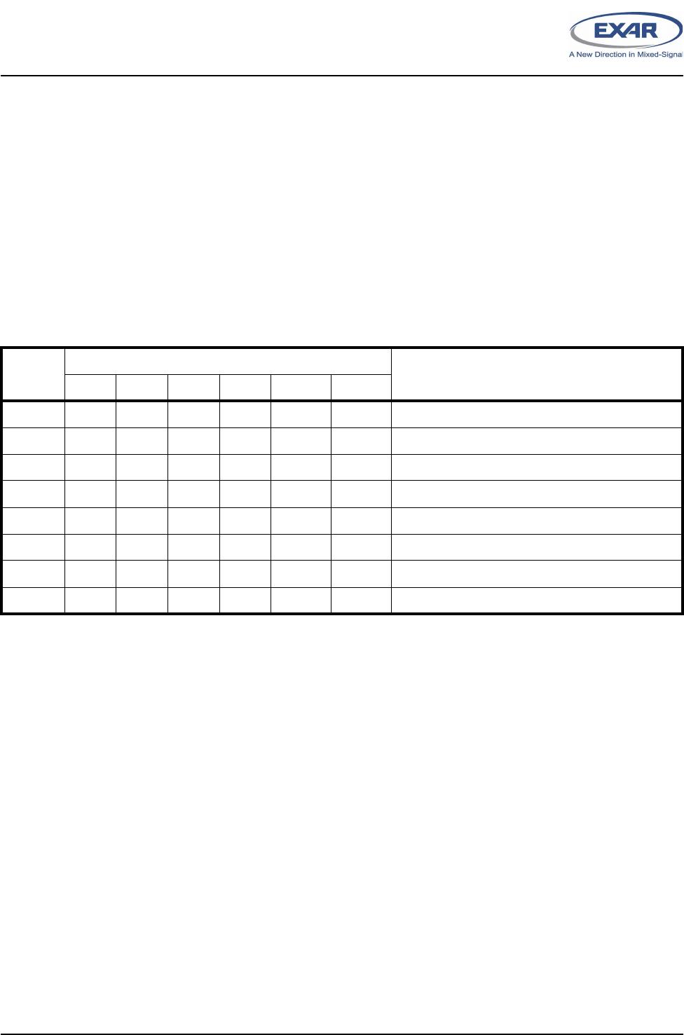
FCR[5:4]: Transmit FIFO Trigger Select
(logic 0 = default, TX trigger level = one)
These 2 bits set the trigger level for the transmit FIFO. The UART will issue a transmit interrupt when the
number of characters in the FIFO falls below the selected trigger level, or when it gets empty in case that the
FIFO did not get filled over the trigger level on last re-load.
Table 11
below shows the selections. EFR bit-4
must be set to ‘1’ before these bits can be accessed. Note that the receiver and the transmitter cannot use
different trigger tables. Whichever selection is made last applies to both the RX and TX side.
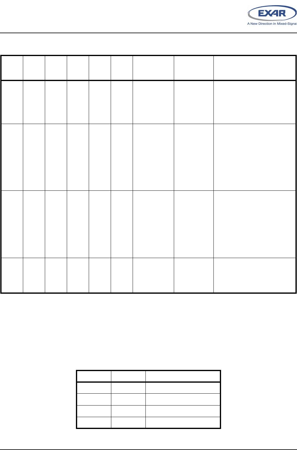
FCR[7:6]: Receive FIFO Trigger Select
(logic 0 = default, RX trigger level =1)
The FCTR Bits 5-4 are associated with these 2 bits. These 2 bits are used to set the trigger level for the receive
FIFO. The UART will issue a receive interrupt when the number of the characters in the FIFO crosses the
trigger level.
Table 11
shows the complete selections. Note that the receiver and the transmitter cannot use
different trigger tables. Whichever selection is made last applies to both the RX and TX side.
XR16C864
30
2.97V TO 5.5V QUAD UART WITH 128-BYTE FIFO
REV. 2.2.0
4.6 Line Control Register (LCR) - Read/Write
The Line Control Register is used to specify the asynchronous data communication format. The word or
character length, the number of stop bits, and the parity are selected by writing the appropriate bits in this
register.
LCR[1:0]: TX and RX Word Length Select
These two bits specify the word length to be transmitted or received.
T
ABLE
11: T
RANSMIT
AND
R
ECEIVE
FIFO T
RIGGER
L
EVEL
S
ELECTION
FCTR
B
IT
-5
FCTR
B
IT
-4
FCR
B
IT
-7
FCR
B
IT
-6
FCR
B
IT
-5
FCR
BIT
-4
R
ECEIVE
T
RIGGER
L
EVEL
T
RANSMIT
T
RIGGER
L
EVEL
C
OMPATIBILITY
0 0
0
0
1
1
0
1
0
1
0 0
1 (default)
4
8
14
1 (default) Table-A. 16C550, 16C2550,
16C2552, 16C554, 16C580
compatible.
0 1
0
0
1
1
0
1
0
1
0
0
1
1
0
1
0
1
8
16
24
28
16
8
24
30
Table-B. 16C650A compatible.
1 0
0
0
1
1
0
1
0
1
0
0
1
1
0
1
0
1
8
16
56
60
8
16
32
56
Table-C. 16C654 compatible.
1 1 X X X X Programmable
via TRG
register.
FCTR[7] = 0.
Programmable
via TRG
register.
FCTR[7] = 1.
Table-D. 16L2750, 16C2850,
16C2852, 16C850, 16C864
compatible.
BIT-1 BIT-0 W
ORD
LENGTH
0 0 5 (default)
0 1 6
1 0 7
1 1 8

XR16C864IQ-F

Mfr. #:
Manufacturer:
MaxLinear
Description:
UART Interface IC UART
Lifecycle:
New from this manufacturer.
Delivery:
DHL FedEx Ups TNT EMS
Payment:
T/T Paypal Visa MoneyGram Western Union

Products related to this Datasheet