ICS1894-40
10BASE-T/100BASE-TX INTEGRATED PHYCEIVER WITH RMII INTERFACE PHYCEIVER
IDT®
10BASE-T/100BASE-TX INTEGRATED PHYCEIVER WITH RMII INTERFACE 10
ICS1894-40 REV K 022412
RMII Signal Definition
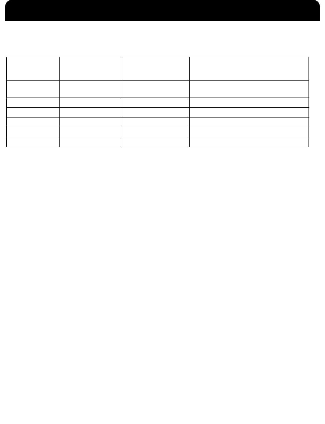
The following table describes the RMII signals. Refer to RMII Specification for detailed information.
Reference Clock (REFIN)
REFIN is sourced by the MAC or system board. It is a
continuous 50MHz clock that provides the timing reference
for TX_EN, TXD[1:0], CRS_DV, RXD[1:0], and RX_ER.
Transmit Enable (TX_EN)
TX_EN indicates that the MAC is presenting di-bits on
TXD[1:0] for transmission. It is asserted synchronously with
the first nibble of the preamble and remains asserted while
all di-bits to be transmitted are presented on the RMII, and
is negated prior to the first REFIN following the final di-bit of
a frame. TX_EN transitions synchronously with respect to
REFIN.
Transmit Data [1:0] (TXD[1:0])
TXD[1:0] transitions synchronously with respect to REFIN.
When TX_EN is asserted, TXD[1:0] are accepted for
transmission by the PHY. TXD[1:0] is ”00” to indicate idle
when TX_EN is de-asserted. Values other than “00” on
TXD[1:0] while TX_EN is de-asserted are ignored by the
PHY.
Carrier Sense/Data Valid (CRS_DV[RXDV])
CRS_DV, identified as RXDV (pin 23), shall be asserted by
the PHY when the receive medium is non-idle. The specifics
of the definition of idle for 10BASE-T and 100BASE-X are
contained in IEEE 802.3 [1] and IEEE 802.3u [2]. CRS_DV
is asserted asynchronously on detection of carrier due to
the criteria relevant to the operating mode. That is, in
10BASE-T mode, when squelch is passed or in 100BASE-X
mode when 2 non-contiguous zeroes in 10 bits are detected
carrier is said to be detected.
Loss of carrier shall result in the deassertion of CRS_DV
synchronous to the cycle of REFIN which presents the first
di-bit of a nibble onto RXD[1:0] (i.e. CRS_DV is deasserted
only on nibble boundaries). If the PHY has additional bits to
be presented on RXD[1:0] following the initial deassertion of
CRS_DV, then the PHY shall assert CRS_DV on cycles of
REFIN which present the second di-bit of each nibble and
deassert CRS_DV on cycles of REFIN which present the
first di-bit of a nibble. The result is: Starting on nibble
boundaries CRS_DV toggles at 25 MHz in 100Mb/s mode
and 2.5 MHz in 10Mb/s mode when the Carrier event ends
before the RX_DV signal internal to the PHY is deasserted
(i.e. the FIFO still has bits to transfer when the carrier event
ends.) Therefore, the MAC can accurately recover RX_DV
and the Carrier event end time. During a false carrier event,
CRS_DV shall remain asserted for the duration of carrier
activity.
The data on RXD[1:0] is considered valid once CRS_DV is
asserted. However, since the assertion of CRS_DV is
asynchronous relative to REFIN, the data on RXD[1:0] shall
be "00" until proper receive signal decoding takes place (see
definition of RXD[1:0] behavior).
*Note: CRS_DV is asserted asynchronously in order to
minimize latency of control signals through the PHY.
Receive Data [1:0] (RXD[1:0])
RXD[1:0] transitions synchronously to REFIN. For each
clock period in which CRS_DV is asserted, RXD[1:0]
transfers two bits of recovered data from the PHY. RXD[1:0]
is "00" to indicate idle when CRS_DV is de-asserted. Values
other than “00” on RXD[1:0] while CRS_DV is de-asserted
are ignored by the MAC.
RMII Signal Name Direction
(with respect to PHY,
ICS1894-40 signal)
Direction
(with respect to MAC)
Description
REFIN Input Input or Output Synchronous 50 MHz clock reference for
receive, transmit and control interface
TX_EN Input Output Transmit Enable
TXD[1:0] Input Output Transmit Data [1:0]
RXD[1:0 Output Input Receive Data [1:0]
RX_ER Output Input, or (not required) Receive Error
CRS_DV[RXDV] Output Input Carrier Sense/Data Valid