ICS1894-40
10BASE-T/100BASE-TX INTEGRATED PHYCEIVER WITH RMII INTERFACE PHYCEIVER
IDT®
10BASE-T/100BASE-TX INTEGRATED PHYCEIVER WITH RMII INTERFACE 13
ICS1894-40 REV K 022412
Crystal or Oscillator Connection
10 pF (optional)
REF_IN
37
REF_OUT
36
CMOS
50.000
MHz
33 Ohm (optional)
NC
ICS1894-40
RMII w/ Oscillator Input
25 pF
REF_IN
37
REF_OUT
36
25.000MHz
25 pF
ICS1894-40
MII w/ Crystal Input
10 pF (optional)
REF_IN
37
REF_OUT
36
CMOS
25.000
MHz
33 Ohm (optional)
NC
MII w/ Oscillator Input
ICS1894-40
NOTE: 25 pF crystal load
capacitors were required to
bring the ppm for the 25 MHz
crystal within the ±50 ppm on
the IDT 1894 PHY evaluation
board. The crystal used had a
recommended load capacitance
of 18 pF.
ICS1894-40
10BASE-T/100BASE-TX INTEGRATED PHYCEIVER WITH RMII INTERFACE PHYCEIVER
IDT®
10BASE-T/100BASE-TX INTEGRATED PHYCEIVER WITH RMII INTERFACE 14
ICS1894-40 REV K 022412
If a crystal is used as the clocking source, connect it to both
the REF_IN (pin 37) and REF_OUT (pin 36) pins of the
ICS1894-40. A pair of bypass capacitors on either side of
the crystal are connected to ground. The crystal is used in
the parallel resonance or anti-resonance mode. The value
of the load caps serve to adjust the final frequency of the
crystal oscillation. Typical applications would use 25 pF load
caps. The exact value will be affected by the board routing
capacitance on REF_IN and REF_OUT pins. Smaller load
capacitors raise the frequency of oscillation.
Once the exact value of load capacitance is established it
will be the same for all boards using the same specification
crystal. The best way to measure the crystal frequency is to
measure the frequency of TXCLK (pin 28) using a frequency
counter with a 1 second gate time. Using the buffered output
TXCLK prevents the crystal frequency from being affected
by the measurement. The crystal specification is shown in
the 25MHz Crystal Specification table.
25 MHz Crystal Specification Table
25 MHz Oscillator Specification table
50 MHz Oscillator Specification table
Status Interface
The ICS1894-40 has five multi-function configuration pins
that report the PHY status by providing signals that are
intended for driving LEDs. Configuration is set by Bank0
Register 20.
Specifications Symbol Minimum Typical Maximum Unit
Fundamental Frequency F0 24.99875 25.00000 25.00125 MHz
Freq. Tolerance
ΔF/f ± 50 ppm
Input Capacitance Cin 3 pF
Specifications Symbol Minimum Typical Maximum Unit
Output Frequency F0 24.99875 25.00000 25.00125 MHz
Freq. Stability (including aging)
ΔF/f ± 50 ppm
Duty cycle CMOS level one-half VDD Tw/T 35 65 %
VIH 2.79 Volts
VIL 0.33 Volts
Specifications Symbol Minimum Typical Maximum Unit
Output Frequency F0 49.9975 50.00000 50.0025 MHz
Freq. Stability (including aging)
ΔF/f ± 50 ppm
Duty cycle CMOS level one-half VDD Tw/T 35 65 %
VIH 2.79 Volts
VIL 0.33 Volts
ICS1894-40
10BASE-T/100BASE-TX INTEGRATED PHYCEIVER WITH RMII INTERFACE PHYCEIVER
IDT®
10BASE-T/100BASE-TX INTEGRATED PHYCEIVER WITH RMII INTERFACE 15
ICS1894-40 REV K 022412
Pins for Monitoring the Data Link table
Note:
1. During either power-on reset or hardware reset, each
multi-function configuration pin is an input that is sampled
when the ICS1894-40 exits the reset state. After sampling is
complete, these pins are output pins that can drive status
LEDs.
2. A software reset does not affect the state of a
multi-function configuration pin. During a software reset, all
multi-function configuration pins are outputs.
3. The P0/LED0 and P1/ISO/LED1 pins must be pulled
either up or down with an external resistor to establish the
address of the ICS1894-40. The P2/INT, P3/RXD2 and
P4/LED2 pins have internal pull-up/ pull-down resistors.
LEDs may be placed in series with these resistors to provide
a designated status indicator as described in the Pins for
Monitoring the Data Link table. Use 1KΩ resistors.
Caution: Pins listed in the Pins for Monitoring the Data Link
table must not float.
4. As outputs, the asserted state of a multi-function
configuration pin is the inverse of the sense sampled during
reset. This inversion provides a signal that can illuminate an
LED during an asserted state. For example, if a
multi-function configuration pin is pulled down to ground
through an LED and a current-limiting resistor, then the
sampled sense of the input is low. To illuminate this LED for
the asserted state, the output is driven high.
5. Adding 10KΩ resistors across the LEDs ensures the PHY
address is fully defined during slow VDD power-ramp
conditions.
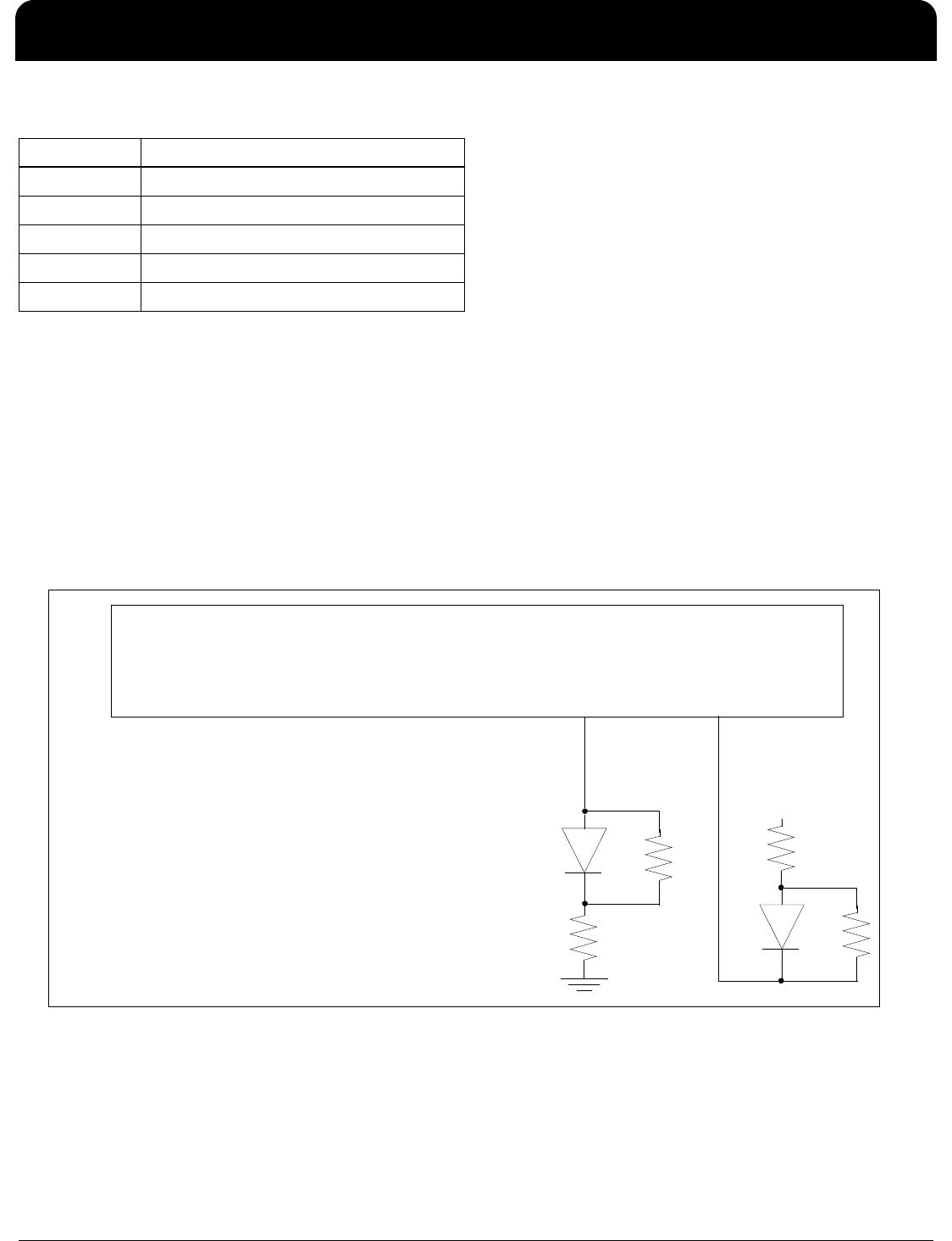
The following figure shows typical biasing and LED connections for the ICS1894-40.
The above circuit decodes the PHY address = 17
Pin LED Driven by the Pin’s Output Signal
P0/LED0 Link, Activity, Tx, Rx, COL, Mode, Dplx
P1/ISO/LED1 Link, Activity, Tx, Rx, COL, Mode, Dplx
P4/LED2 Link, Activity, Tx, Rx, COL, Mode, Dplx
LED3 Link, Activity, Tx, Rx, COL, Mode, Dplx
SI/LED4 Link, Activity, Tx, Rx, COL, Mode, Dplx
ICS1894-40
38
19 12 40 39
P4/LED2
(always
latched high)
P3/RXD2 P2/INT P1/ISO/LED1 P0/LED0
LED0
1KΩ
10KΩ
VDD
LED1
1KΩ
10KΩ

1894K-40LFT

Mfr. #:
Manufacturer:
IDT
Description:
Ethernet ICs 3.3V 10/100 PHY RMII
Lifecycle:
New from this manufacturer.
Delivery:
DHL FedEx Ups TNT EMS
Payment:
T/T Paypal Visa MoneyGram Western Union

Products related to this Datasheet