ICS1894-40
10BASE-T/100BASE-TX INTEGRATED PHYCEIVER WITH RMII INTERFACE PHYCEIVER
IDT®
10BASE-T/100BASE-TX INTEGRATED PHYCEIVER WITH RMII INTERFACE 31
ICS1894-40 REV K 022412
DC Operating Characteristics for Supply Current
The table below lists the DC operating characteristics for the supply current to the ICS1894-40 under various
conditions.
Deep Power Down Current Consumption Table
Condition VDDIO (V) VDD and VDDD (V) Current (mA) (typical)
Autonegotiation 3.3 3.3 68
1.8 3.3 66
100BaseTX FD and Linked 3.3 3.3 102
10BaseTX FD and Linked 3.3 3.3 97
Power Down (Reg0:11 = 1) 3.3 3.3 16
Case 1 Case 2 Case 3 Case 4 Case 5
Register 24:8 DPD Enable
Register 24:7 TPLL_100 DPD Enable
Register 24:6 RX_100 DPD Enable
Register 24:5 Admix_TX DPD Enable
Register 24:4 CDR100_cdr DPD Enable
Current (mA) (typical) 68 39 26 24 16
ICS1894-40
10BASE-T/100BASE-TX INTEGRATED PHYCEIVER WITH RMII INTERFACE PHYCEIVER
IDT®
10BASE-T/100BASE-TX INTEGRATED PHYCEIVER WITH RMII INTERFACE 32
ICS1894-40 REV K 022412
DC Operating Characteristics for Inputs and Outputs
Unless otherwise specified, the table below lists the 3.3V/1.8 V DC operating characteristics of the ICS1894-40
inputs and outputs.
For 3.3 V Signals
For 1.8 V Signals
Parameter Symbol Conditions Min. Max. Units
Input High Voltage V
IH
2.0 V
Input Low Voltage V
IL
–0.8V
Output High Voltage V
OH
I
OH
= –4 mA 2.4 V
Output Low Voltage V
OL
I
OL
= +4 mA 0.4 V
Parameter Symbol Conditions Min. Max. Units
Input High Voltage V
IH
0.8 V
Input Low Voltage V
IL
–0.7V
Output High Voltage V
OH
I
OH
= –4 mA 1.6 V
Output Low Voltage V
OL
I
OL
= +4 mA 0.1 V
ICS1894-40
10BASE-T/100BASE-TX INTEGRATED PHYCEIVER WITH RMII INTERFACE PHYCEIVER
IDT®
10BASE-T/100BASE-TX INTEGRATED PHYCEIVER WITH RMII INTERFACE 33
ICS1894-40 REV K 022412
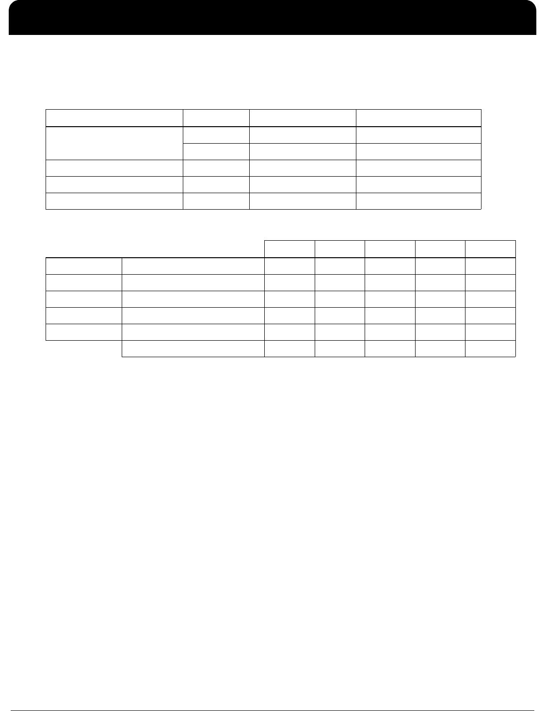
DC Operating Characteristics for REF_IN
The table below lists the 3.3V DC characteristics for the REF_IN pin.
DC Operating Characteristics for MII Pins
The table below lists DC operating characteristics for the Media Independent Interface (MII) for the ICS1894-40.
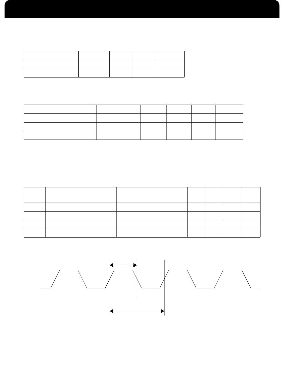
Timing Diagrams
Timing for Clock Reference (REF_IN) Pin
The table below lists the significant time periods for signals on the clock reference (REF_IN) pin. The REF_IN
Timing Diagram figure shows the timing diagram for the time periods.
REF_IN Timing Diagram
Parameter Symbol Min. Max. Units
Input High Voltage V
IH
2.97 V
Input Low Voltage V
IL
–0.33 V
Parameter Conditions Min. Typ. Max. Units
MII Input Pin Capacitance 8 pF
MII Output Pin Capacitance 14 pF
MII Output Drive Impedance VDDIO = 3.3V 20 Ω
Time
Period
Parameter Conditions Min. Typ. Max. Units
t1 REF_IN Duty Cycle (MII) 45 50 55 %
t2 REF_IN Period (MII) 40 ns
t1 REF_IN Duty Cycle (RMII) 45 50 55 %
t2 REF_IN Period (RMII) 20 ns
REF_IN
t1
t2

1894K-40LFT

Mfr. #:
Manufacturer:
IDT
Description:
Ethernet ICs 3.3V 10/100 PHY RMII
Lifecycle:
New from this manufacturer.
Delivery:
DHL FedEx Ups TNT EMS
Payment:
T/T Paypal Visa MoneyGram Western Union

Products related to this Datasheet