ICS1894-40
10BASE-T/100BASE-TX INTEGRATED PHYCEIVER WITH RMII INTERFACE PHYCEIVER
IDT®
10BASE-T/100BASE-TX INTEGRATED PHYCEIVER WITH RMII INTERFACE 43
ICS1894-40 REV K 022412
100M MII Media Independent Interface: Receive Latency
The table below lists the significant time periods for the 100M MII/100M Stream Interface receive latency. The time
periods consist of timings of signals on the following pins:
TP_RX (that is, TP_RXP and TP_RXN)
RXCLK
RXD (that is, RXD[3:0])
The 100M MII/100M Stream Interface: Receive Latency Timing Diagram shows the timing diagram for the time
periods.
100M MII/100M Stream Interface: Receive Latency Timing Diagram
Time
Period
Parameter Conditions Min. Typ. Max. Units
t1 First Bit of /J/ into TP_RX to /J/ on RXD 100M MII 16 17 Bit times
RXCLK
TP_RX
Shown
unscrambled.
RXD
t1
ICS1894-40
10BASE-T/100BASE-TX INTEGRATED PHYCEIVER WITH RMII INTERFACE PHYCEIVER
IDT®
10BASE-T/100BASE-TX INTEGRATED PHYCEIVER WITH RMII INTERFACE 44
ICS1894-40 REV K 022412
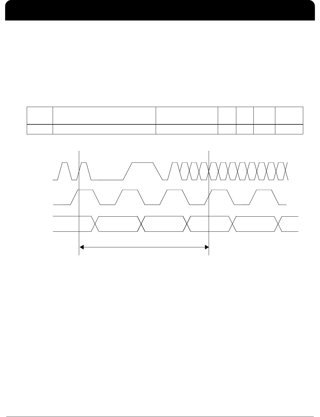
100M Media Independent Interface: Input-to-Carrier Assertion/De-Assertion
The table below lists the significant time periods for the 100M MDI input-to-carrier assertion/de-assertion. The time
periods consist of timings of signals on the following pins:
TP_RX (that is, TP_RXP and TP_RXN)
CRS
COL
The 100M MDI Input to Carrier Assertion/De-Assertion Timing Diagram shows the timing diagram for the time
periods.
The IEEE maximum is 20 bit times.
The IEEE minimum is 13 bit times, and the maximum is 24 bit times.
100M MDI Input to Carrier Assertion/De-Assertion Timing Diagram
Time
Period
Parameter Conditions Min. Typ. Max. Units
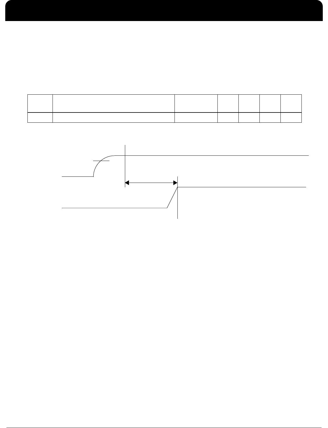
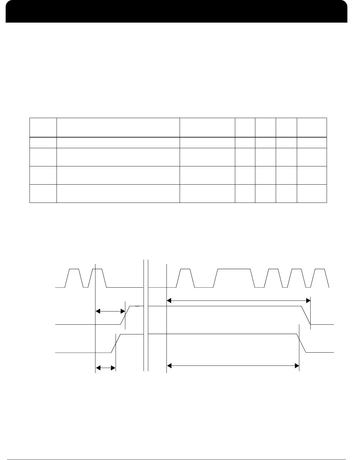
t1 First Bit of /J/ into TP_RX to CRS Assert † 10 14 Bit times
t2 First Bit of /J/ into TP_RX while
Transmitting Data to COL Assert †
Half-Duplex Mode 9 13 Bit times
t3 First Bit of /T/ into TP_RX to CRS
De-Assert ‡
–1318Bit times
t4 First Bit of /T/ Received into TP_RX to
COL De-Assert ‡
Half-Duplex Mode 13 18 Bit times
t1
t2
t3
t4
First bit First bit of /T/
Shown
unscrambled.
TP_RX
CRS
COL
ICS1894-40
10BASE-T/100BASE-TX INTEGRATED PHYCEIVER WITH RMII INTERFACE PHYCEIVER
IDT®
10BASE-T/100BASE-TX INTEGRATED PHYCEIVER WITH RMII INTERFACE 45
ICS1894-40 REV K 022412
Reset: Power-On Reset
The table below lists the significant time periods for the power-on reset. The time periods consist of timings of
signals on the following pins:
VDD
TXCLK
The Power-On Reset Timing Diagram shows the timing diagram for the time periods.
Power-On Reset Timing Diagram
Time
Period
Parameter Conditions Min. Typ. Max. Units
t1 VDD 2.7 V to Reset Complete 40 45 500 ms
TXCLK
Valid
VDD
2.7 V
t1

1894K-40LFT

Mfr. #:
Manufacturer:
IDT
Description:
Ethernet ICs 3.3V 10/100 PHY RMII
Lifecycle:
New from this manufacturer.
Delivery:
DHL FedEx Ups TNT EMS
Payment:
T/T Paypal Visa MoneyGram Western Union

Products related to this Datasheet