ICS1894-40
10BASE-T/100BASE-TX INTEGRATED PHYCEIVER WITH RMII INTERFACE PHYCEIVER
IDT®
10BASE-T/100BASE-TX INTEGRATED PHYCEIVER WITH RMII INTERFACE 50
ICS1894-40 REV K 022412
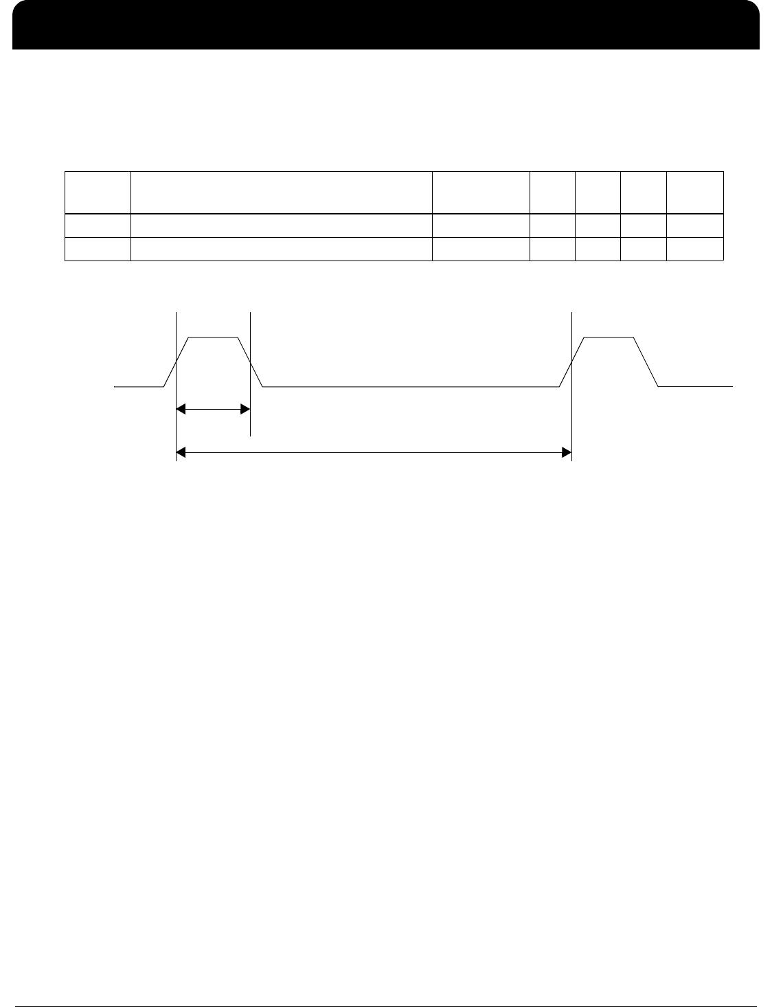
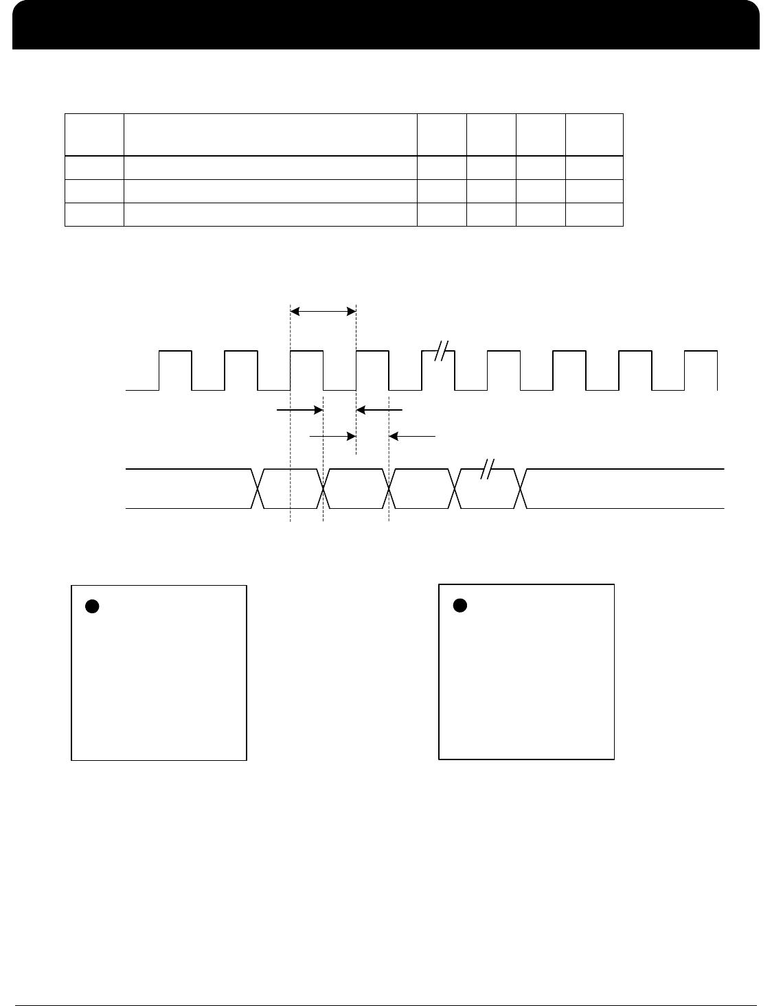
Auto-Negotiation Fast Link Pulse Timing
The table below lists the significant time periods for the ICS1894-40 Auto-Negotiation Fast Link Pulse. The time
periods consist of timings of signals on the following pins:
• TP_TXP
• TP_TXN
The Auto-Negotiation Fast Link Pulse Timing Diagram shows the timing diagram for one pair of these differential
signals, for example TP_TXP minus TP_TXN.
Auto-Negotiation Fast Link Pulse Timing Diagram
Time
Period
Parameter Conditions Min. Typ. Max. Units
t1 Clock/Data Pulse Width – – 90 – ns
t2 Clock Pulse-to-Data Pulse Timing – 55 60 70 μs
t3 Clock Pulse-to-Clock Pulse Timing – 110 125 140 μs
t4 Fast Link Pulse Burst Width – – 5 – ms
t5 Fast Link Pulse Burst to Fast Link Pulse Burst – 10 15 25 ms
t6 Number of Clock/Data Pulses in a Burst – 15 20 30 pulses
Clock
Pulse
Clock
Pulse
Data
Pulse
t1
t3
t2
t4
t5
t1
FLP Burst FLP Burst
Differential
Twisted Pair
Transmit Signal
Differential
Twisted Pair
Transmit Signal