Tsi721 Datasheet 18 April 4, 2016
Integrated Device Technology
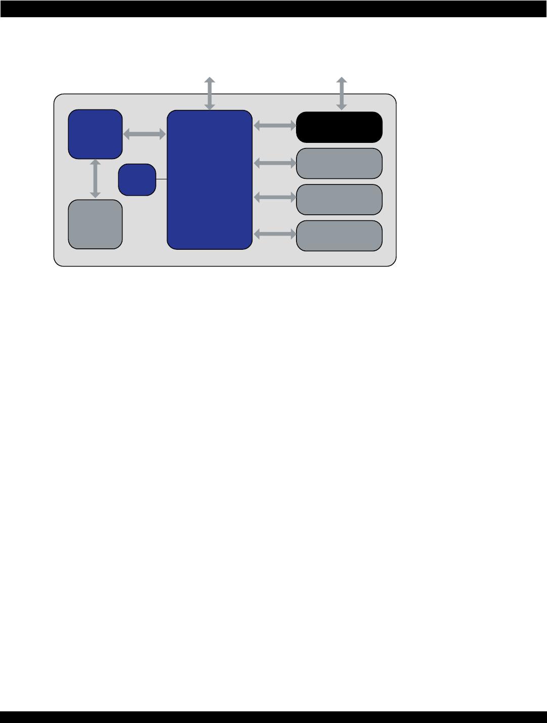
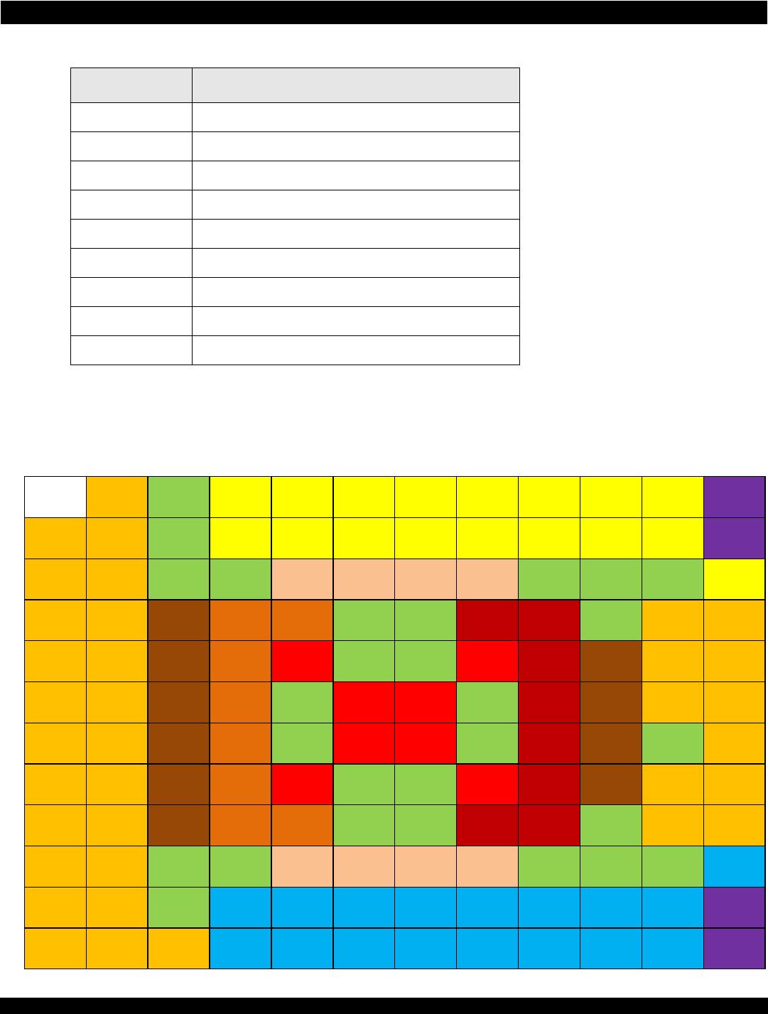
2.2 Ballmap
Figure 5: Ballmap
IO-PD 3.3/2.5V LVTTL Bidirectional with Pull-down
IO-PU 3.3/2.5V LVTTL Bidirectional with Pull-up
PCIE_O Differential CML PCIe output
PCIE_I Differential CML PCIe input
SRIO_O Differential CML S-RIO output
SRIO_I Differential CML S-RIO input
DIFF_I Differential CML input
PWR Power
GND Ground
Table 1: Signal Types (Continued)
Pin Type Definition
123456789101112
A
NO_BALL GPIO[9] VSS PCRP[0] PCTP[0] PCTP[1] PCRP[1] PCRP[2] PCTP[2] PCTP[3] PCRP[3] PCCLKP
B
GPIO[0] GPIO[10] VSS PCRN[0] PCTN[0] PCTN[1] PCRN[1] PCRN[2] PCTN[2] PCTN[3] PCRN[3] PCCLKN
C
GPIO[1] GPIO[11] VSS VSS AVDD25 AVDD25 AVDD25 AVDD25 VSS VSS VSS PCBIAS
D
GPIO[2] GPIO[12] VDDIO AVTT AVTT VSS VSS AVDD10 AVDD10 VSS TDO PCRSTOn
E
GPIO[3] GPIO[13] VDDIO AVTT VDD VSS VSS VDD AVDD10 VDDIO TCK TEST_BCE
F
GPIO[4] GPIO[14] VDDIO AVTT VSS VDD VDD VSS AVDD10 VDDIO TDI TEST_ON
G
GPIO[5] GPIO[15] VDDIO AVTT VSS VDD VDD VSS AVDD10 VDDIO VSS
TEST_BIDIR_CT
L
H
GPIO[6] STRAP_RATE[0] VDDIO AVTT VDD VSS VSS VDD AVDD10 VDDIO TMS RSTn
J
GPIO[7] STRAP_RATE[1] VDDIO AVTT AVTT VSS VSS AVDD10 AVDD10 VSS TRSTn SRRSTOn
K
GPIO[8] STRAP_RATE[2] VSS VSS AVDD25 AVDD25 AVDD25 AVDD25 VSS VSS VSS SRBIAS
L
I2C_SCL CLKMOD VSS SRRN[0] SRTN[0] SRTN[1] SRRN[1] SRRN[2] SRTN[2] SRTN[3] SRRN[3] REFCLKN
M
I2C_SDA MECS SR_BOOT SRRP[0] SRTP[0] SRTP[1] SRRP[1] SRRP[2] SRTP[2] SRTP[3] SRRP[3] REFCLKP