Tsi721 Datasheet 43 April 4, 2016
Integrated Device Technology
3.7.4 Level I Long Run Transmitter Specifications
1. For all Load Types: R_Rdin = 100 Ohm +/- 20 Ohm.
2. Load Type 0 with min. T_Vdiff, AC-coupling or floating load.
3. It is suggested that T_SCC22 be -6 dB to be compatible with Level II transmitter requirements.
4. It is suggested that T_Ncm be limited to 5% of T_Vdiff to be compatible with Level II transmitter requirements.
For each baud rate at which the LP-Serial transmitter is specified to operate, the output eye pattern of the transmitter falls
entirely within the unshaded portion of the Transmitter Output Compliance Mask displayed in Figure 7 when measured at the
output pins of the device and the device is driving a 100 Ohm + 5% differential resistive load. The specification allows the
output eye pattern of a LP-Serial transmitter that implements pre-emphasis (to equalize the link and reduce inter-symbol
interference) to only comply with the Transmitter Output Compliance Mask when pre-emphasis is disabled or minimized.
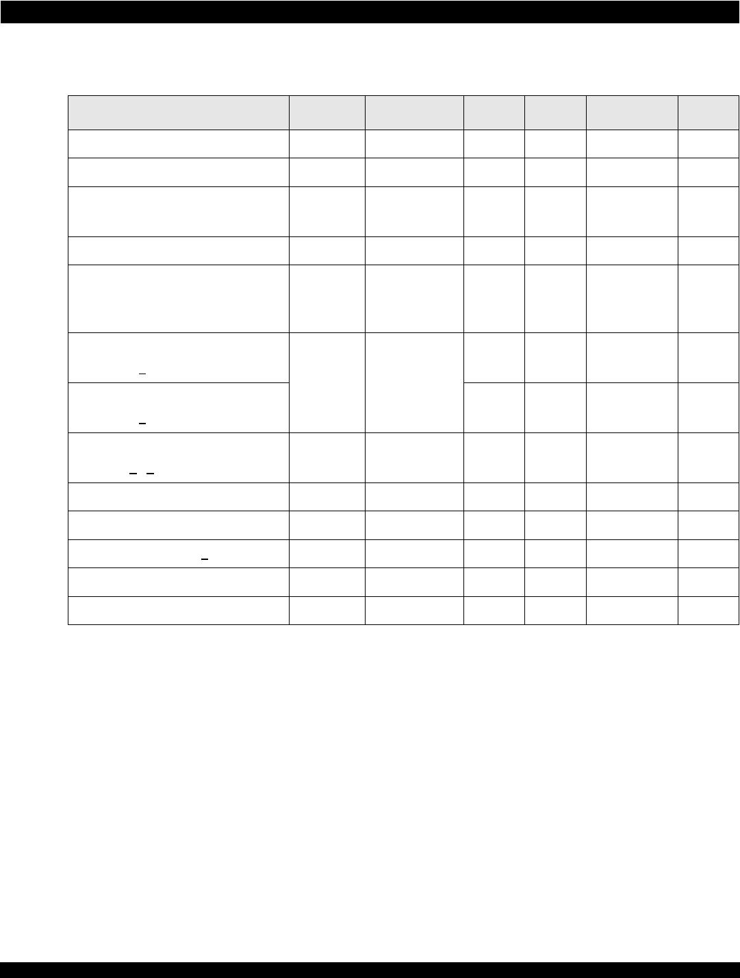
Table 21: Level I Long Run Transmitter AC Timing Specifications
Characteristics Symbol Reference Min Typ Max Units
Baud Rate T_Baud Section 9.4.2.2 1.25 - 3.125 Gbps
Absolute Output Voltage V
O
Section 9.4.2.3 -0.40 - 2.30 Volts
Output Differential Voltage
(into floating load Rload = 100 Ohm)
T_Vdiff Section 9.4.2.3 800 - 1600 mVppd
Differential Resistance T_Rd Section 9.4.1.5 80 100 120 Ohm
Recommended output rise and fall
times
(20% to 80%)
T_tr, T_tf - 60 - - ps
Differential Output Return Loss
(T_baud/10 <
f < T_baud/2)
T_SDD22 Section 9.4.1.6 - - - dB
Differential Output Return Loss
(T_baud/10 <
f < T_baud/2)
-- - dB
Common Mode Return Loss
(625 MHz <
f < T_baud)
T_TCC22 Section 9.4.1.6 - - Note 3 dB
Transmitter Common Mode Noise
1
T_Ncm - - Note 4 mVppd
Output Common Mode Voltage T_Vcm Load Type 0
2
0- 2.1 V
Multiple output skew, N <
4S
MO
---1000ps
Multiple output skew, N > 4 S
MO
- - - 2UI + 1000 ps
Unit Interval UI - 80 - 800 ps
Tsi721 Datasheet 44 April 4, 2016
Integrated Device Technology
Figure 7: S-RIO Transition Symbol Transmit Eye Mask
Table 22: Level I Near-End (Tx) Template Intervals
Characteristic Symbol
Near-End
SR Value
Near-End
LR Value
Units
Eye mask T_X1 0.17 0.17 UI
Eye mask T_X2 0.39 0.39 UI
Eye mask T_Y1 250 400 mV
Eye mask T_Y2 500 800 mV
Eye mask T_Y3 N/A N/A mV
Uncorrelated bounded high
probability jitter
T_UBHPJ 0.17 0.17 UIpp
Duty cycle distortion T_DCD 0.05 0.05 UIpp
Total jitter T_TJ 0.35 0.35 UIpp
Tsi721 Datasheet 45 April 4, 2016
Integrated Device Technology
3.7.4.0.1 Level I Receiver Specifications
Level I LP-Serial receiver electrical and timing specifications are stated in the text and tables of this section.
1. Input common mode voltage for AC-coupled or floating load input with min. T_Vdiff.
2. Receiver is required to implement at least one of the specified nominal R_Vtt values, and usually implements only one of
these values. Receiver is only required to meet R_Vrcm parameter values that correspond to R_Vtt values supported.
3. Input common mode voltage for AC-coupled or floating load input with min. T_Vdiff.
4. For floating load, input resistance must be > 1K Ohm.
Table 23: Level I Receiver Electrical Input Specifications
Characteristic Symbol Reference Minimum Typical Maximum Units
Rx baud rate (1.25 Gbps) R_Baud - - 1.250 - Gbps
Rx baud rate (2.5 Gbps) - - 2.500 - Gbps
Rx baud rate (3.125 Gbps) - - 3.125 - Gbps
Absolute input voltage R_Vin Section
9.4.3.4
----
Input differential voltage R_Vdiff Section
9.4.3.3
200 - 1600 mVppd
Differential resistance R_Rdin Section
9.4.3.7
80 100 120 Ohm
Differential input return loss
(100 MHz <
f < R_Baud/2)
R_SDD11 Section
9.4.3.7
---dB
Differential input return loss
(R_Baud/2 <
f < R_Baud)
----
Common mode input return loss
(625 MHz <
f < T_baud)
R_SCC11 Section
9.4.3.7
---dB
Termination voltage
1,2
R_Vtt R_Vtt
floating
4
Not specified V
Input common mode voltage
1,2
R_Vrcm R_Vtt
floating
3,4
-0.05 - 1.85 V
Wander divider n - - 10 - -

TSI721A1-16GILV

Mfr. #:
Manufacturer:
IDT
Description:
PCI Interface IC PCIe-to-Rapid IO Bridge
Lifecycle:
New from this manufacturer.
Delivery:
DHL FedEx Ups TNT EMS
Payment:
T/T Paypal Visa MoneyGram Western Union