Tsi721 Datasheet 50 April 4, 2016
Integrated Device Technology
2. Load Type 0 with min T_Vdiff, AC-Coupling or floating load.
3. For load Type 1 through 3: R_Zvtt < 30 Ohm; Vtt is defined for each load type as follows: Load Type 1 R_Vtt = 1.2V +5% / -
8%; Load Type 2 R_Vtt = 1.0V +5% / -8%; Load Type 3 R_Vtt = 0.8V +5% / -8%.
4. DC Coupling compliance is optional (Type 1 through 3). Only Transmitters that support DC coupling are required to meet this
parameter. It is acceptable for a transmitter to restrict the range of T_Vdiff in order to comply with the specified T_Vcm range.
For a transmitter which supports multiple T_Vdiff levels, it is acceptable for a transmitter to claim DC Coupling Compliance
if it meets the T_Vcm ranges for at least one of its T_Vdiff setting as long as those setting(s) that are compliant are indicated.
5. Simple CML transmitters designed using VDD > 1.2V can still claim DC compliance if this parameter is not met.
6. Simple CML transmitters designed using VDD < 0.8V can still claim DC compliance if this parameter is not met.
1. The transmitter must be able to produce a minimum T_Vdiff greater than or equal to 800mVppd. In applications where the
channel is better than the worst case allowed, a Transmitter device can be provisioned to produce T_Vdiff less than this
minimum value, but greater than or equal to 400mVppd, and is still compliant with this specification.
2. Load Type 0 with min T_Vdiff, AC-Coupling or floating load.
3. For load Type 1: R_Zvtt < 30 Ohm; T_Vtt and R_Vtt = 1.2V +5% / - 8%.
4. DC coupling compliance is optional (Load Type 1). Only Transmitters that support DC coupling are required to meet this
parameter.
3.7.4.3.3 Level II Medium Transmitter Specifications
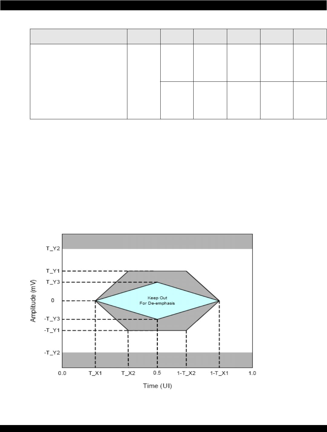
Table 27: Level II Medium Run Transmitter Output Electrical Specifications
Characteristic Symbol Reference Minimum Typical Maximum Units
Baud rate (5 Gbps) T_Baud Section
10.4.2.1.2
5.00
-0.01%
5.00 5.00
+0.01%
Gbps
Absolute output voltage V
O
Section
10.4.2.1.3
-0.40 - 2.30 Volts
Output differential voltage
(into floating load Rload = 100 Ohm)
T_Vdiff Section
104.2.1.3
1
800 - 1200 mVppd
Differential resistance T_Rd Section
10.4.2.1.6
80 100 120 Ohm
Recommended output rise and fall
times (20% to 80%)
T_tr, T_tf Section
10.4.2.1.4
30 - - ps
Differential output return loss
(100 MHz to 0.5 *T_Baud)
T_SDD22 Section
10.4.2.1.6
---8dB
Differential output return loss
(0.5*T_Baud to T_Baud)
---dB
Common mode return loss
(100 MHz to 0.75 *T_Baud)
T_TCC22 Section
10.4.2.1.6
---6dB
Transmitter common mode noise T_Ncm - - - 5% of
T_Vdiff
mVppd