Tsi721 Datasheet 57 April 4, 2016
Integrated Device Technology
3.7.5 Reference Clocks – PCCLKP/N and REFCLKP/N
Table 32 lists the PCCLKP/N and REFCLKP/N clock electrical characteristics of the Tsi721.
PCCLKP/N and REFCLKP/N require a terminated, DC biased, differential clock source. This type of reference clock is usually
used in PCIe systems but not in S-RIO systems. Different clock technologies can be used with the Tsi721 provided that proper
termination is used.
The following diagrams provide examples of commonly used clock technologies connected to PCCPLKP/N and REFCLKP/N.
The clock source that drives the PCCLK inputs must meet all requirements for the common clock
architecture defined for the reference clock in the PCI Express Base Specification (Rev. 2.1).
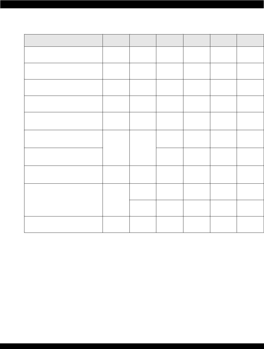
Table 32: PCCLKP/N and REFCLKP/NClock Electrical Characteristics
Symbol Parameter Minimum Typical Maximum Unit
V
IN_DIFF
Differential input voltage (single-ended peak
to peak)
0.3 - 1.0 V
V
DC
Input level 0 - 2.5 V
V
CM
a
a. Common-mode voltage must be supplied by the clock source circuit.
Common-mode input level 0.15 - 2.0 V
F
REFCLK
REFCLK clock frequency 100 - 156.25 MHz
S
REFCLK
REFCLK stability -100 - +100 ppm
TJ
REFCLK
REFCLK total phase jitter (1 MHz–20 MHz) - - 1 ps (rms)
F
PCCLK
PCCLK clock frequency 100 - 156.25 MHz
S
PCCLK
PCCLK average frequency accuracy -300 - 300 ppm
CCJ
PCCLK
PCCLK cycle-to-cycle jitter - - 150 ps
F
DUTY
Clock duty cycle 40 - 60 %
T
ER-RISE
Rising edge rate 0.6 - - V/ns
T
ER-FALL
Falling edge rate 0.6 - - V/ns
Zin
b
b. Clock termination must be implemented on the circuit board.
Clock input impedance - High - Ohm