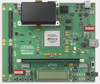
Intel®'s Stratix® III FPGA Development Kit delivers a complete environment for the development and testing of designs requiring high-performance and high-density devices.
The Stratix III FPGAs combine the world's highest performance and highest density with the lowest possible power consumption. You'll find Stratix III FPGAs provide the high-performance and high-integration capabilities needed for next-generation basestations, network infrastructure, and advanced imaging equipment.
Specifically designed for ease of use and rapid system integration, the Stratix III FPGA family offers two family variants optimized to meet different application needs:
- The Stratix III L family provides balanced logic, memory, and multiplier ratios for mainstream applications.
- The Stratix III E family is memory and multiplier rich for data-centric applications. Modular I/O banks with a common bank structure for vertical migration lend efficiency and flexibility to the high speed I/O. Package and die enhancements with dynamic on-chip termination, output delay, and current strength control provide best-in-class signal integrity.
Stratix III devices offer the following features:
- 48,000 to 338,000 equivalent logic elements (LEs)
- 2,430 to 20,497 Kbits of enhanced TriMatrix memory consisting of three RAM block sizes to implement true dual-port memory and first-in first-out (FIFO) buffers
- High-speed DSP blocks provide dedicated implementation of 9×9, 12×12, 18×18, and 36×36 multipliers (at up to 550 MHz), multiply-accumulate functions, and finite impulse response (FIR) filters
- I/O:GND:PWR ratio of 8:1:1 along with on-die and on-package decoupling for robust signal integrity
- Programmable Power Technology, which minimizes power while maximizing device performance
- Selectable Core Voltage, available in low-voltage devices (L ordering code suffix), enables selection of lowest power or highest performance operation
- Up to 16 global clocks, 88 regional clocks, and 116 peripheral clocks per device
- Up to 12 phase-locked loops (PLLs) per device that support PLL reconfiguration, clock switchover, programmable bandwidth, clock synthesis, and dynamic phase shifting
- Memory interface support with dedicated DQS logic on all I/O banks
- Support for high-speed external memory interfaces including DDR, DDR2, DDR3 SDRAM, RLDRAM II, QDR II, and QDR II+ SRAM on up to 24 modular I/O banks
- Up to 1,104 user I/O pins arranged in 24 modular I/O banks that support a wide range of industry I/O standards
- Dynamic On-Chip Termination (OCT) with auto calibration support on all I/O banks
- High-speed differential I/O support with serializer/deserializer (SERDES) and dynamic phase alignment (DPA) circuitry for 1.25 Gbps performance
- Support for high-speed networking and communications bus standards including SPI-4.2, SFI-4, SGMII, Utopia IV, 10 Gigabit Ethernet XSBI, Rapid I/O and NPSI
- The only high-density, high-performance FPGA with support for 256-bit (AES) volatile and non-volatile security key to protect designs
- Robust on-chip hot socketing and power sequencing support
- Integrated cyclical redundancy check (CRC) for configuration memory error detection with critical error determination for high availability systems support
- Built-in error correction coding (ECC) circuitry to detect and correct data errors in M144K TriMatrix memory blocks
- Nios® II embedded processor support
- Support for multiple intellectual property megafunctions from Intel FPGA Intellectual Property (IP) functions.
The Stratix III FPGA Development Kit is RoHS compliant and includes:
- Stratix III development board
- Stratix III EP3SL150F1152 high-performance FPGA
- 142,500 equivalent logic elements (LEs)
- 744 user I/O pins
- 384 18 x 18 multipliers
- Clocking
- 125.000-MHz oscillator
- 50.000-MHz oscillator
- SMA input
- SMA output
- Configuration
- MAX® II flash passive serial configuration circuit
- MAX II EPM2210GF256C3N CPLD
- 2,210 LEs
- 272 user I/O pins
- 8 Kbytes of user flash memory
- On-board USB-Blaster™ using Quartus® II development software programming
- JTAG download port
- General user input/output
- Power consumption display
- Displays each power rail individually
- System reset pushbutton
- Board-specific DIP switch
- JTAG bypass DIP switch
- User reset pushbutton
- User pushbuttons (x4)
- User DIP switch (x8)
- User LEDs (x8)
- User quad 7-segment display
- 128 x 64 dot pixels graphics display
- LCD (16 character x 2 line)
- Memory devices
- 128-Mbyte DDR2 SDRAM DIMM
- 16-Mbyte DDR2 SDRAM devices (individually addressable)
- 36-Mbit QDRII SRAM device
- 4-Mbyte PSRAM
- 64-Mbyte flash memory
- Components and interfaces
- USB 2.0
- 10/100/1000 Ethernet
- Two HSMC interfaces
- Power supplies
- 12A DC/DC µModule - LTM4601EV
- 1.5A low input voltage VLDO linear regulator - LTC3026EDD
- 100-mA, low noise, LDO micropower regulators in SOT-23 - LT1761ES5-SD
- 4.5A, 500-kHz step-down switching regulator - LT1374CFE
- 1.2-MHz/2.2-MHz inverting DC/DC converters in ThinSOT - LT1931AES5
- 1-/2-channel 24-bit µPower no latency delta-sigma ADC in MSOP-10 - LTC2402CMS
- Quartus II Development Kit Edition software, including a one-year license
- Cable and accessories
- External AC adapter power supply
- Power cord (including support for UK, Europe)
