By Analog Devices Inc 51
ADI's ADA4622 is the next generation of the AD822 single-supply, rail-to-rail output (RRO), precision, JFET-input op amp. The ADA4622 includes many improvements that make it desirable as an upgrade without compromising the flexibility and ease of use that makes the AD822 useful for a wide variety of applications. The input voltage range includes the negative supply and the output swings rail-to-rail. Input EMI filters are added to increase the signal robustness in the face of closely located, switching noise sources.
The speed, in terms of bandwidth and slew rate, is increased along with a strong output drive to improve settling time performance and enable the device to drive the inputs of modern, single-ended successive approximation register analog-to-digital converters (SAR ADCs).
Voltage noise is reduced, both broadband by 25% and 1/f by half, while holding the supply current constant. DC precision is improved over the AD822 with half the offset and a maximum thermal-drift specification is added to the ADA4622. The common-mode rejection ratio is improved over the AD822 to make the ADA4622 more suitable than the AD822 when used in noninverting gain and difference amplifier configurations.
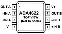
The ADA4622 is specified for operation over the extended industrial-temperature range of -40°C to +125°C and operates from 5 V to 30 V with specifications at +5 V, ±5 V, and ±15 V. The ADA4622 is available in 8-lead SOIC and 8-lead MSOP packages.