By Analog Devices Inc 69
ADI’s AD9164 DACs are high performance, 16-bit, DDS devices that support update rates to 6 GSPS. The DAC core is based on a quad-switch architecture coupled with a 2x interpolator filter that enables an effective DAC update rate of up to 12 GSPS in some modes. The high dynamic range and bandwidth makes these DACs ideally suited for the most demanding high speed RF DAC applications. The DDS consists of a bank of thirty-two, 32-bit numerically controlled oscillators (NCOs), each with its own phase accumulator. When combined with a 100 MHz serial peripheral interface (SPI) and fast hop modes, phase coherent fast frequency hopping (FFH) is enabled, with several modes to support multiple applications.
In baseband mode, wide analog bandwidth capability combines with high dynamic range to support Data Over Cable Service Interface Specifications DOCSIS 3.1 cable infrastructure compliance from the minimum of one carrier up to the full maximum spectrum of 1.791 GHz of signal bandwidth. A 2x interpolator filter (FIR85) enables the AD9164 to be configured for lower data rates and converter clocking to reduce the overall system power and ease the filtering requirements. In Mix-Mode™ operation, the AD9164 can reconstruct RF carriers in the second and third Nyquist zones up to 7.5 GHz while still maintaining exceptional dynamic range. The output current can be programmed from 8 mA to 38.76 mA. The AD9164 data interface consists of up to eight JESD204B serializer/deserializer (SERDES) lanes that are programmable in terms of lane speed and number of lanes to enable application flexibility.
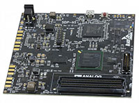
An SPI configures the AD9164 and monitors the status of all registers. The AD9164 is offered in 165-ball and 169-ball CSP_BGA packages.
| Features | ||
|
|
|
| Applications | ||
|
|