By Cypress Semiconductor Corp 64
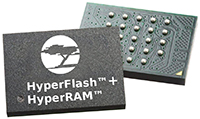
The Cypress HyperFlash™ and HyperRAM™ multi-chip package (MCP) is a solution that combines a high-speed NOR Flash memory for fast-boot, instant-on capability with a self-refresh DRAM for expanded scratchpad memory in a reduced footprint, (measuring 8 mm by 6 mm) low-pin-count package in a 24 BGA. This complete NOR Flash/DRAM memory subsystem, based on the Cypress HyperBus™ interface, is the ideal solution for space-constrained and cost-optimized IoT and embedded designs.
The HyperFlash and HyperRAM MCP leverages Cypress’ 12-pin HyperBus™ interface that shares a common footprint with both discrete HyperFlash and HyperRAM products. This common footprint enables design engineers to implement a single-pad layout that supports either a discrete device or the HyperFlash and HyperRAM MCP, allowing changes at any point in the design or product lifecycle without affecting the board layout. This flexibility enables differentiated end products based on a single platform design, saving development time and minimizing cost. It reduces pin count by 70% and offers a 77% space savings compared to competing SDRAM and Quad SPI memory solutions.
The HyperFlash and HyperRAM MCP is the ideal solution for a wide range of embedded applications like automotive clusters and infotainment, communications equipment, industrial applications, and high-performance consumer products. The product is offered in an industrial-plus (-40°C to 105°C) temperature range.