By STMicroelectronics 402
SG3525 is an integrated circuit chip commonly used to design and control switching power supply systems, especially for DC to AC inverter applications. It is a PWM (Pulse Width Modulation) controller that generates pulse signals used to control switching power supply switches.

SG3525 is a single-chip integrated PWM control chip with excellent performance, comprehensive functions, and is easy to operate and flexible to use. The output adopts push-pull output mode, which enhances the driving performance of the system; it has a built-in under-voltage locking circuit and soft Start-up control circuit, PWM latch, with over-current protection, adjustable frequency, and ability to limit maximum duty cycle.
SG3525 is a current-controlled PWM controller whose pulse width is adjusted according to the connected feedback current. At the input end of the pulse width comparator, the signal flowing through the output inductor coil is directly compared with the error amplifier output signal, thereby adjusting the duty cycle so that the output inductor peak current changes with the change of the error voltage. The voltage loop-current loop double-loop structure improves the switching power supply in terms of voltage regulation, load regulation and transient response. It is an ideal new control method.
Ⅰ.Main features and functions of SG3525
•Dual output: SG3525 usually has two PWM output pins, which can be used to control the positive and negative half-bridge circuits of the switching power supply respectively.
•PWM control: SG3525 can effectively control the output voltage and frequency of the switching power supply by adjusting the width of the output pulse. This makes it ideal for designing stable inverters and DC power supplies.
•Operating voltage range: 8-35V
•Internal error amplifier: SG3525 has a built-in error amplification circuit that can be compared with the reference voltage to stabilize the output voltage.
•With external oscillator synchronization function
•Oscillator operating frequency range: 100HZ-400KHz
•With input under-voltage lockout function
•External capacitor for frequency modulation: The frequency of PWM output can be adjusted by connecting an external capacitor.
•Built-in soft start circuit
•Overcurrent protection: SG3525 usually has an overcurrent protection function, which can shut down the output to protect the circuit when the current exceeds the safe range.
•Dead time adjustable
•Over-temperature protection: It also usually has over-temperature protection to prevent the chip from overheating.
•With PWM memory function, multiple pulses are prohibited
•Pulse-by-pulse shutdown
•Input voltage range: The SG3525 is usually able to operate within a certain range, usually between 12V and 40V.
•Dual output (sink/source): mA (peak).
•External pins: SG3525 chips usually have multiple pins, including PWM output, reference voltage input, error amplifier input and feedback input, etc.
Ⅱ. Pin functions and working principle of SG3525
Pin:
1.Inv.input (Pin 1): Inverting input terminal of error amplifier. In a closed loop system, this pin is connected to the feedback signal. In an open-loop system, this end is connected to the compensation signal input end (pin 9) to form a follower.
2.Noninv.input (Pin 2): Non-inverting input terminal of error amplifier. In closed loop systems and open loop systems, this terminal is connected to the given signal. Depending on the needs, different types of feedback networks can be connected between this end and the compensation signal input end (pin 9) to form proportional, proportional-integral and integral regulators.
3.Sync (pin 3): The oscillator is externally connected to the synchronization signal input terminal. This terminal is connected to an external synchronization pulse signal to achieve synchronization with the external circuit.
4.OSC.Output (pin 4): oscillator output.
5.CT (pin|pin 5): oscillator timing capacitor access terminal.
6.RT (Pin 6): Oscillator timing resistor access terminal.
7.Discharge (pin 7): oscillator discharge terminal. An external discharge resistor is connected between this end and pin 5 to form a discharge circuit.
8.Soft-Start (pin 8): Soft-start capacitor access terminal. This end is usually connected to a 5 soft-start capacitor.
9.Compensation(pin 9): PWM comparator compensation signal input terminal. Different types of feedback networks are connected between this end and pin 2 to form proportional, proportional integral and integral regulators.
10.Shutdown (pin 10): External shutdown signal input. The controller output is disabled when this terminal is tied high. This end can be connected to the protection circuit to achieve fault protection.
11.Output A (Pin 11): Output A. Pin 11 and pin 14 are two complementary output terminals.
12.Ground (pin 12): signal ground.
13.Vc (pin 13): Output stage bias voltage access terminal.
14.Output B (Pin 14): Output terminal B. Pin 14 and pin 11 are two complementary output terminals.
15.Vcc (Pin 15): Bias power input terminal.
16.Vref (pin 16): reference power output. This terminal can output a reference voltage with excellent temperature stability.

Working principle:
SG3525 has a built-in 5.1V precision reference power supply, which is fine-tuned to 1.0%. Within the common-mode input voltage range of the error amplifier, there is no need for an external voltage divider. SG3525 has a synchronization function, which can realize master-slave working mode and synchronization with external clock signals, providing great flexibility for design. Adding a resistor between the CT pin and the Discharge pin can adjust the dead time. Since SG3525 integrates a soft-start circuit, only one external timing capacitor is needed.
The soft-start access terminal (pin 8) of SG3525 is usually connected to a 5 soft-start capacitor. During the power-on process, since the voltage across the capacitor cannot change suddenly, the reverse input terminal of the PWM comparator connected to the access terminal of the soft-start capacitor is at low level, and the PWM comparator outputs high level. At this time, the output of the PWM register is also high level, and the high level is added to the output transistor through two NOR gates, making it impossible to conduct.
SG3525 contains an error amplifier internally, which compares the reference voltage with the feedback voltage and generates an error signal. The error signal represents the difference between the output voltage and the desired voltage. The SG3525 typically has one or more PWM output pins for connection to the control circuit of a switching power supply. PWM signals are output through these pins to control switching devices (such as MOSFETs or IGBTs) on and off.
The external shutdown signal affects both the output stage and the soft-start circuit. When the signal on Shutdown (pin 10) is high, the PWM register will act immediately to prohibit the output of SG3525. At the same time, the soft-start capacitor will begin to discharge. If the high level continues, the soft-start capacitor will be fully discharged, and the soft-start process will not be re-entered until the shutdown signal ends.
The undervoltage lockout function also acts on the output stage and soft-start circuit. If the input voltage is too low, the soft-start capacitor will start to discharge while the output of SG3525 is turned off.
Ⅳ.SG3525 controlled switching power supply
1. Connect the SG3525 chip: First, connect the SG3525 chip to the circuit correctly. This includes providing the appropriate supply voltage and ground, as well as connecting the chip's PWM output pins and other necessary pins.
2. Set the reference voltage: In order to control the output voltage, a reference voltage needs to be provided. This reference voltage is usually related to the desired output voltage. Connect the reference voltage to the corresponding pin of the SG3525.
3. Feedback loop: Switching power supplies usually have a feedback loop that measures the actual output voltage and feeds it back to the SG3525.
4. PWM signal generation: SG3525 will generate a PWM signal based on the feedback signal and reference voltage. The duty cycle of the PWM signal will be adjusted based on the difference between the actual output voltage and the desired output voltage.
5. Connect the PWM output: Connect the pulse width modulation output pin of the SG3525 to the control pin of the gate or switching element such as MOSFET, IGBT. The switching device uses PWM signals to switch the power supply.
V. Structural design of SG3525
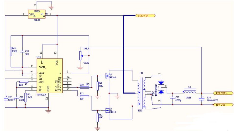
The power input voltage is provided by a +30V power supply with an isolation transformer, and the DC-AC inverter converter schematic diagram designed by SG3525 is used. The performance indicators are: the input voltage is DC24~35V adjustable, the input rated voltage is 30V, and the output is 5V/lA.
This system uses SG3525 to generate two reverse square waves to control the on and off of MOSFET. The MOSFET driver adopts push-pull mode. This design adds 30V DC voltage to the center tap of the transformer, and the output part adopts full-wave rectification. At the output point There is a voltage dividing resistor to provide a reference voltage to TL431, and it is fed back to SG3525 through photoelectric isolation to adjust and control the output square wave duty cycle to stabilize the output voltage.
Ⅵ.Efficiency of SG3525 in inverter circuit
1. Output filtering: The output of the inverter power supply is generally a square wave or PWM waveform, and this signal may contain higher frequency noise. Using a suitable output filter circuit can effectively reduce the harmonic components in the output waveform, improve the quality of the output voltage, and also improve the working efficiency of the circuit.
2. Switching device efficiency: Inverter circuits usually use switching devices (such as MOSFETs or IGBTs) to control the switching of current. The efficiency of these switching devices has a great impact on the efficiency of the entire circuit. Selection of high-efficiency switching devices and appropriate heat dissipation measures can improve efficiency.
3. Inductor and capacitor selection: Inverter circuits usually require inductors and capacitors to filter and stabilize the output voltage. Selecting appropriate inductor and capacitor values can affect efficiency.
4. Load characteristics: The load characteristics of the inverter circuit (such as load size and nature) also affect efficiency. Circuits may exhibit different efficiencies under different load conditions.
5. Thermal and temperature management: Keeping switching devices and circuits within the appropriate temperature range to avoid overheating is critical to maintaining high efficiency.
Frequently Asked Questions
1.What is the difference between SG3525AN and SG3525?
Models with the letters "AN" suffix usually indicate that the chip is an industrial or military-grade product, while models without the suffix may be general commercial-grade products. Therefore, SG3525AN is generally designed for more harsh environments and applications with higher reliability and tolerance. Industrial or military grade chips typically have a wider operating temperature range and can operate in a wider range of temperature conditions, while commercial grade chips may have a narrower temperature range.
2.How to adjust the output frequency of SG3525?
The frequency of SG3525 can be adjusted by external capacitor. Typically, a capacitor is connected to the corresponding pin of the SG3525 (usually Pin 5 and Pin 6) to control the frequency. The output frequency of SG3525 is inversely proportional to the connected capacitor value. Connect the selected capacitor to the corresponding pin of the SG3525. Make sure the capacitors are connected correctly to avoid circuit problems.
3.How to deal with troubleshooting and common problems of SG3525 chip?
Make sure the power supply of the SG3525 chip is within the specified operating range and the power supply voltage is stable. Unstable or insufficient supply voltage may cause the chip to operate improperly. Check the external components related to the SG3525 chip, such as capacitors, inductors, resistors, etc., to ensure that their values and connections are correct. Check whether the reference voltage used by the chip is correct. If the reference voltage is unstable or incorrect, it may cause output problems.