By NXP Semiconductors 224
A shift register is a device that uses sequential logic to store and transfer binary data. A shift register is a bidirectional circuit that moves each bit of data from input to output on each clock pulse. There are currently a variety of shift register models, among which the 74HC595 is such a serial-parallel output shift register.
74HC595 is an integrated circuit chip that belongs to the 74 series of logic integrated circuits. It is an 8-bit shift register commonly used to expand the digital output ports of microcontrollers. The "74" in its name indicates that it belongs to the TTL (Transistor-Transistor Logic) logic family, while the "HC" indicates high-speed CMOS (Complementary Metal Oxide Semiconductor) technology. The 74HC595 allows data to be shifted bit-by-bit into internal memory via a serial input and then output in parallel to one or more of the 8 output pins.
74HC595 is an 8-bit serial input, parallel output displacement register: the parallel output is a three-state output. At the rising edge of SCK, the serial data is input from SDL to the internal 8-bit shift register and output by Q7, while the parallel output stores the data in the 8-bit shift register into 8 bits at the rising edge of LCK. Parallel output buffer. When the control signal of the serial data input terminal OE is low enable, the output value of the parallel output terminal is equal to the value stored in the parallel output buffer.

Ⅰ.Specification parameters of 74HC595
•Typical tpd:13ns
•Wide operating voltage:2-6V
•Operating temperature range:0°C to 70°C
•Maximum clock frequency:25Mhz @4.5V
•Output voltage high level (VOH):close to VCC
•Output voltage low level (VOL):close to 0V
•Input voltage low level (VIL):0-20% VCC
•Input voltage high level (VIH):70-80% VCC
•Supply voltage (VCC):Typical value is 3.3V or 5V
•Output current low level (IOL):in the range of several milliamps (mA)
•Output current low level (IOL):in the range of several milliamps (mA)
•Input capacity (Cin):unit is picofarad (pF)
•Output capacity (Cout):unit is picofarad (pF)
•Input current low level (IIL):very low, measured in microamps (μA)
•Input current high level (IIH):very low, measured in microamps (μA)
•Packaging:Available in a variety of packages, including 16-pin GDIP, PDIP and PDSO
Ⅱ.Working principle of 74HC595
1.Data input:Data is input serially through the serial input pin (SER). Normally, the lowest bit of data (the rightmost bit) is entered first.
2.Storage register:There is an 8-bit storage register inside the 74HC595. Under the control of the clock signal, it receives the input data bit by bit and stores the data into the storage register in parallel in the next clock cycle. When the rising edge of a clock signal arrives, the input data is moved into the storage register, and at the same time, the data in the storage register is also output in parallel. In this way, the storage register acts as a buffer so that the input data can be read bit by bit. Reception and processing, while output data can also be driven in parallel.
3.Shift register:74HC595 also has a shift register, which can convert serial input data into parallel output. This shift register shifts out the input data bit by bit under the control of the clock signal, and clocks the The rising edge of the cycle stores data into the storage register in parallel.
4.Clock control:The clock signal is provided by the clock input pin (SRCLK). Each time a clock pulse is generated, the next bit of input data is shifted into the storage register.
5.Parallel output:After all 8-bit data are input and stored in the storage register, the contents of the storage register can be output in parallel to the 8 outputs through a pulse called the storage register clock input pin (RCLK or LATCH) one or more of the pins.
6.Clear function:74HC595 also usually has a clear input pin (MR or CLR), which is used to clear the data in the storage register.
Ⅲ.Recommended operating conditions of 74HC595
In accordance with the Absolute Maximum Rating System (IEC 60134);voltages are referenced to GND(ground=0 V)

Ⅳ.AC WAVEFORMS of 74HC595
74HC595: VM= 50%.VI= GND to VCC


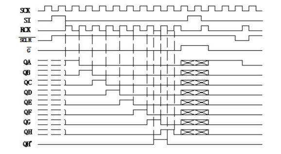
Ⅴ.Sequence diagram of 74HC595
Ⅵ. Precautions for 74HC595
1.Supply voltage stability: Ensure a stable supply voltage for the 74HC595 to avoid adverse effects of voltage fluctuations on its performance. Use power supply capacitors to smooth the voltage.
2.Clock pulse: Control the frequency and timing of the clock signal to ensure correct data shifting and storage. The rising or falling edge of the clock signal may be used for data shifting, depending on the model of the 74HC595.
3.Input level: Ensure that the input signal level is within the specified input level range. Typically, the input level high (VIH) and the input level low (VIL) are a percentage of the supply voltage.
4.Data shift sequence: Pay attention to the data shift sequence of 74HC595, which is usually from the lowest bit (rightmost) to the highest bit (leftmost), but the specifics may vary depending on the model.
5.Output current and load: Understand the maximum current capability of the 74HC595's output pin and ensure that the external load does not exceed the specified range.
6.Cascade connection: If you cascade multiple 74HC595 chips, make sure you connect the clock and serial output pins correctly so that the data shifts correctly in the cascade.
7.ESD Protection: When handling and connecting the 74HC595, take anti-static measures to prevent damage to the chip from electrostatic discharge (ESD).
Ⅶ.Processing serial to parallel conversion of 74HC595 data signal
1.Serial input data: Input the data to be converted to the serial input pin (SER) of 74HC595 in serial mode. Normally, the lowest bit of data is entered first.
2.Storage register: There is an 8-bit storage register inside the 74HC595, which is used to temporarily store input data. This storage register accepts input data bit by bit under the control of a clock signal.
3.Storage register clock pulse: In order to output the data in the storage register in parallel, you need to generate a storage register clock pulse. This is usually done via the storage register clock input pin (RCLK or LATCH). The generation of the storage register clock pulse indicates that all 8 bits of data have been input and stored.
4.Parallel output: Once the storage register clock pulse is triggered, the data in the storage register will be output in parallel to one or more of the 8 output pins. The state of the output pin (high or low) will be set based on the value of the corresponding bit in the storage register.
Frequently Asked Questions
1.74What is the voltage range of HC595?
Voltage levels range from 0 to Vcc, where Vcc is typically 4.75V - 5.25V. Voltage range 0V - 0.8V creates logic level 0. Voltage range 2V - Vcc creates logic level 1. The 74HC595 is an 8-bit serial input, serial or parallel output shift register with an output latch.
2.What is the function of 74HC595?
The 74HC595 is a high speed CMOS device. The eight-bit shift register accepts data from the serial input (DS) on each positive transition of the shift register clock (SHCP). When asserted low, the reset function sets all shift register values to zero and is independent of all clocks.
3.What are some common applications of the 74HC595?
Common applications include driving LED displays, controlling multiple LEDs, driving 7-segment displays, and interfacing with various digital output devices.
4.What's the maximum output current for each output pin on a 74HC595?
The maximum output current per pin typically ranges from 4 to 6 mA, depending on the specific model.