By Texas Instruments 191
74LS04 is an integrated circuit composed of 6 inverters. Each inverter has an input and an output. Each channel of the 74LS04 (that is, each inverter) has two input terminals and an output terminal. When the input terminal receives a high level (usually 5V or higher voltage), the output terminal will output a low voltage. level (usually 0V or lower voltage); conversely, when the input terminal receives a low level, the output terminal will output a high level.
The 74LS04 is TTL/CMOS based, which allows the device to be used more reliably with other microcontroller TTL devices. Such chips can be used in circuits to perform a variety of tasks. For example, if you need an inverted version of a signal, you can use one channel of the 74LS04. If you need to amplify the signal strength, you can use 74LS04 in combination with other logic gates such as AND, OR, NAND, NOR, etc. For example, you can use an AND gate and a NOT gate (such as one channel of the 74LS04) to create a NOR gate, a very common gate in digital logic.
Ⅰ.Function of 74LS04
The 74LS04 is a six-channel inverter (Inverter) used to perform logical inversion operations on input signals. In more detail, it converts input logic levels, that is, high (1) is input into high (1) and low (0) is input. This is the main function of the 74LS04.
This feature is very useful in digital electronic circuits because it can be used to perform signal inversion, signal amplification, logic gate cascades, and other logic operations. Generally, logic inverters are basic building blocks in digital circuit design and are used to build various complex logic functions.
If a high-level signal (1) is input to an input pin of the 74LS04, the corresponding output pin will produce a low-level signal (0). Conversely, if a low-level signal (0) is input to it, the output will become a high-level signal (1).
Ⅱ.Power consumption of 74LS04
The 74LS04 has low power consumption, which depends on input and output frequency and current. It should be noted that although the power consumption of a single 74LS04 chip may not be high, when multiple such chips are used in complex circuits or used together with other high-power consumption chips, the total power consumption of the entire system may become higher. . Therefore, when designing electronic devices, especially mobile devices or battery-powered devices, the circuit should be optimized as much as possible to reduce total power consumption.
The specific power consumption value will be affected by the following factors:
1.Operating voltage: Power consumption usually increases as the operating voltage increases, because at high voltages, the current will also increase accordingly.
2.Clock frequency: When operating at a faster speed, the device will require higher power consumption for logic inversion.
3.Output Load: Loads (e.g., resistors, other logic gates) connected to the 74LS04 outputs will affect power consumption. Heavier loads may require more current to maintain output levels.
4.Temperature: Ambient temperature also affects power consumption, and power consumption usually increases slightly at high temperatures.
Ⅲ.Features of 74LS04
1.Operating voltage range: 74LS04 typically operates within the operating voltage range of 4.75V to 5.25V, which makes it suitable for standard TTL supply voltages.
2.Standard TTL input and output: 74LS04 follows standard TTL logic level standards, with clearly defined high-level and low-level voltage thresholds.
3.Common digital circuit building blocks: 74LS04 is one of the common basic building blocks in digital electronic circuits and can be used to build various logic circuits, including signal inversion, signal amplification, logic gate cascades, etc.
4.Low latency: 74LS04 has relatively low logic latency and is suitable for applications that require fast response.
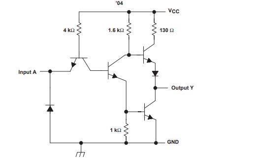
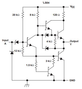
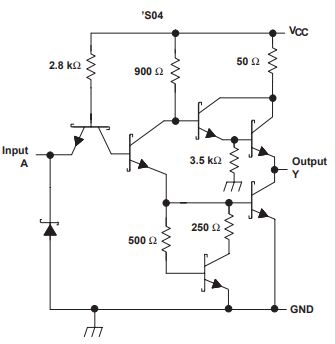
IV.74LS04 schematics
V.Specifications of 74LS04
•Operating voltage range: 4.75V to 5.25V
•Input voltage high level (VIH): 2.0V to 5.25V
•Output voltage high level (VOH): 2.7V (minimum) to Vcc (supply voltage)
•Input voltage low level (VIL): 0V to 0.8V
•Output voltage low level (VOL): 0.5V or less
•Input current: 1μA
•Operating temperature range: 0°C-70°C
•Package type: DIP, SOIC
Ⅵ.Working principle and application fields of 74LS04
•Working principle
1.Working principle: Each inverter uses a bipolar transistor internally to implement logical inversion operation. When the input pin receives a high signal (1), internal circuitry causes the output pin to generate a low signal (0). When the input pin receives a low level signal (0), the output pin will generate a high level signal (1). This inverting operation is achieved by turning the transistor on and off.
2.Input and output: The 74LS04 has six identical inverters, each with an input pin and an output pin. Each input pin can be connected to a logic high (1) or logic low (0), while the corresponding output pin will produce the opposite logic level of the input. That is, a high level input will produce a low level output, and a low level input will produce a high level output.
3.Cascade connection: Multiple 74LS04 inverters can be connected in cascade to perform more complex logic operations. For example, if you connect the output of one 74LS04 to the input of another 74LS04, you will get two inversions, which is the logic value of the original input. This makes the 74LS04 very useful for building a variety of digital logic circuits.
•Application areas
1.Digital electronics education and experimentation: 74LS04 is an ideal tool for learning digital logic and electronics. It is used in education and laboratory experiments to help students understand logical inversion operations and digital circuit principles.
2.Communication equipment: 74LS04 can be used to process digital signals and circuits, such as modems, communication interfaces, signal processing, etc.
3.Digital logic circuit design: 74LS04 is often used to build digital logic circuits, such as sequential circuits, counters, multiplexers and decoders. It can be used to perform operations such as signal inversion, signal amplification, and logic gate cascading.
4.Automation and control systems: 74LS04 can be used to perform logical control operations, including processing of switches, sensor inputs and executing logical decisions.
5.Embedded systems: 74LS04 is widely used in embedded systems to process input and output signals, perform logical operations and control external devices. It can be used in interface circuits, status indicators, logic controllers, etc.
6.Digital display and LED control: 74LS04 can be used to drive digital displays, LEDs and other digital indicators to display various information.
7.Instruments and measuring equipment: Among various instruments and measuring equipment, 74LS04 can be used for logic control, signal processing and data acquisition.
8.Computer hardware: In computer hardware, 74LS04 can be used to perform various logical operations, including address decoding, data processing, and control signal processing.
Ⅶ.74LS04 pin configuration

1.1A: Input pin of the first inverter.
2.1Y: Output pin of the first inverter.
3.2A: Input pin of the second inverter.
4.2Y: Output pin of the second inverter.
5.3A: Input pin of the third inverter.
6.3Y: Output pin of the third inverter.
7.GND (Ground): Ground pin, connected to the ground of the circuit.
8.4Y: Output pin of the fourth inverter.
9.3A: Input pin of the fourth inverter.
10.3Y: Output pin of the fourth inverter.
11.2A: Input pin of the fifth inverter.
12.2Y: Output pin of the fifth inverter.
13.1Y: Output pin of the sixth inverter.
14.Vcc (Supply Voltage): Positive power supply pin, usually connected to the supply voltage (such as +5V).
Frequently Asked Questions
1.What is the difference between 74LS04 and other types of logic gates (such as AND gates and OR gates)?
Differences in logic operations: 74LS04 inverts the input logic level, that is, high-level input becomes low-level output, and low-level input becomes high-level output. The AND gate performs a logical AND operation, and the output is high only when all inputs are high. The OR gate performs a logical OR operation, and as long as one input is high, the output is high. Difference in number of inputs: The 74LS04 has one input per inverter, whereas AND and OR gates typically have two or more inputs.
2.What is the function of 74LS04 hexadecimal inverter?
The 74LS04 six-inverter has 6 independent gates, each performing a logical INVERT function. The output signals of the six inverters are opposite to the input signals. The inverter can reverse the phase of the input signal by 180 degrees.
3.What kind of door is 74LS04?
The 74 series are digital logic integrated circuits. The 74LS04 IC has six NOT gates. These NOT gates perform the inverting function. Hence the name "hexagonal reversal door".
4.Where can 74LS04 be used?
This chip is basically used wherever a logic inverter is required. The inverter gate in this chip provides an output that is the opposite of the logic input. When TTL output is required. Gates in this chip provide TTL logic outputs, which are required in some applications.