By Texas Instruments 179
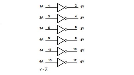
SN7406N is a six-channel inverter integrated circuit chip, often referred to as a six-inverter chip. It is a digital logic gate integrated circuit produced by Texas Instruments. Each inverter has an input pin and an output pin that performs the logical inversion operation. When the input signal is high (1), the output is low (0). This kind of chip is usually used for signal inversion operations in digital logic circuits, or for the construction of other logic gates, such as AND gates, OR gates, NOR gates, etc.
Each inverter in the SN7406N has an input pin and an output pin, which are opposite in logic level. This kind of chip is often used in digital logic circuits for tasks such as signal inversion, timing control, and level conversion. By combining SN7406N with other logic gate chips (such as AND gates, OR gates, etc.), more complex digital logic circuits can be constructed to meet different application needs. It is widely used in digital circuit design, especially in microprocessor systems and other digital systems.
Ⅰ.Main parameters of SN7406N
•Number of input lines:6 Input
•Number of output lines:6 Output
•Polarity:Inverting
•High level output current:-250 uA
•Low level output current:40 mA
•Supply voltage-Max:5.25 V
•Supply voltage-Minimum:4.75 V
•Operating power supply current:51 uA
•Minimum operating temperature:0°C
•Maximum operating temperature:+70°C
•Installation style:SMD/SMT
•Height:3.3mm
•Number of channels:5
•Operating power supply voltage:4.75V to 5.25V
•Quiet current:32.0 mA
•Voltage node:5.00 V
•Mounting type:Through hole
Ⅱ.Features of SN7406N
•DIP package: SN7406N is usually packaged in DIP (Dual In-Line Package), which is easy to insert into a standard socket or breadboard for easy experimentation and prototype design.
•Six-channel inverter: SN7406N contains six independent inverters inside. Each inverter can perform a logic inversion operation and invert the logic level of the input signal.
•Open-Collector Drivers for Indicator Lamps and Relays
•Power supply voltage range: This chip provides different power supply voltage options to adapt to different application needs, usually 3.3V, 5V or 15V power supply voltage.
•Low power consumption: It usually has relatively low power consumption and is suitable for battery-powered or energy-saving applications.
•Convert TTL Voltage Levels to MOS Level
Ⅲ.SN7406N application scenarios
1.Level conversion: When one level needs to be converted to another level, SN7406N can be used as a level converter. It can convert 5V logic level to 3.3V logic level, or perform other level conversion operations. This conversion is useful for connecting devices with different logic level standards, such as when connecting a 5V microprocessor to a 3.3V memory or I/O device. Please note that for this application, voltage compatibility and signal amplitude need to be carefully considered to avoid hardware damage or signal quality degradation.
2.Signal inversion: The most common use is to invert the logic level of the input signal. The SN7406N comes in handy when switching from one logic level to its opposite state is required. One of the main applications of the SN7406N is signal inversion. As mentioned before, it is an inverter buffer/driver whose basic function is to receive a logic level signal and output that signal at the opposite logic level. This signal inversion feature is useful in many applications, such as in digital circuits when a signal needs to be converted from one logic level to another, or when the logic state of one signal needs to be inverted to trigger another equipment or components. At the same time, because the SN7406N has the ability to withstand high current, it can also be used to drive larger loads.
3.Timing control: In timing control circuits, SN7406N can be used to generate control signals, such as the opposite or complementary signals of clock signals. This is useful for timing synchronization and timing operations.
4.Pulse generation: With appropriate configuration, SN7406N can be used to generate pulse signals, such as in timing measurement, frequency analysis, signal modulation, etc. By generating pulse signals with different frequencies and duty cycles, the performance of a circuit can be accurately measured or data transmission can be achieved in communication systems. It should be noted that in order to generate a stable pulse signal, a power supply with sufficient current driving capability needs to be used to power the SN7406N.
5.Signal processing: In digital signal processing systems, SN7406N can be used for signal conditioning and processing to meet specific system requirements.
6.Digital logic operations: SN7406N can be used with other digital logic gate integrated circuits to build complex digital logic circuits, such as multiplexers, frequency dividers, frequency dividers, etc.
7.Digital circuit prototyping: For academic laboratories, prototyping or educational purposes, the SN7406N can be used to build digital circuit prototypes to help students and engineers learn digital circuit design.
Ⅳ.Logic diagram (positive logic) of SN7406N
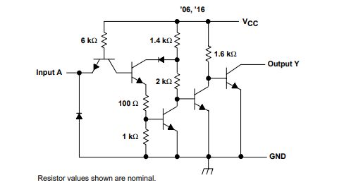
Ⅴ.SN7406N schematic (each buffer/driver)
Ⅵ. Precautions in circuit design of SN7406N
1.Input level: The input signal should meet standard logic level standards. For SN7406N, usually the low level (logic 0) must be within the specified voltage range, and the high level (logic 1) must be within the specified voltage range.
2.Power supply voltage: Make sure that the power supply voltage of SN7406N meets the requirements of the chip specifications. Do not exceed or fall below the specified voltage range.
3.Input current: Consider the input current of SN7406N. Although it is usually small, in some applications the input current may be a consideration, especially if level shifting is required.
4.Noise and anti-interference: Consider signal noise and anti-interference in the design to ensure that the SN7406N can work stably. Use appropriate filtering and shielding methods to reduce noise and interference in circuits.
5.Load capacity: Ensure that the output signal can normally drive the load connected to the SN7406N output pin. If the load is too heavy, it may be necessary to use a signal buffer or amplifier to boost the output signal.
6.Input protection: If the input of the SN7406N is subject to external interference or voltage peaks, it may be necessary to add an input protection circuit to protect the chip from damage.
7.Operating temperature: SN7406N has a specific operating temperature range. Make sure it works properly within the temperature range of the designed operating environment. If the operating temperature exceeds the specified range, chip performance may be affected.
8.Power consumption: Consider the power consumption of SN7406N, especially in power bank or battery-powered applications. Understand the static and dynamic power consumption of the chip in order to optimize the energy efficiency of the circuit.
9.Pin layout: The pins of the chip need to be connected correctly to ensure that the signal is transmitted correctly. Note the input and output pin connections of the inverter.
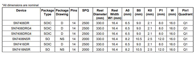
Ⅶ.TAPE AND REEL INFORMATION

Frequently Asked Questions
1.What are the functions of SN7406N?
The main function of the SN7406N is to perform a logic inversion operation. It changes the logic level of the input signal from high to low, or from low to high. SN7406N can be used for digital signal processing, including signal inversion, timing control, level conversion, etc. It has a wide range of uses in digital circuit design.
2.How many pins does SN7406N have?
SN7406N is a six-channel inverter chip. Each inverter has two pins, one input pin and one output pin. Therefore, the SN7406N has a total of 6 inverters, each with 2 pins, for a total of 12 pins.
3.What alternative models are there for SN7406N?
Alternative models of SN7406N include: 74LS04,74HC04,74F04,74AC04